
Key Insights
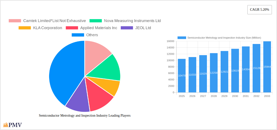
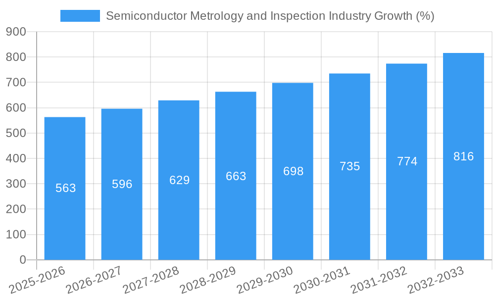
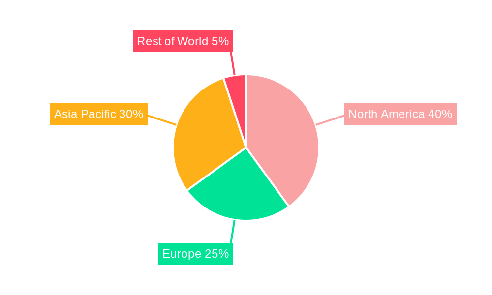
The Semiconductor Metrology and Inspection market, valued at $10.47 billion in 2025, is poised for robust growth, exhibiting a Compound Annual Growth Rate (CAGR) of 5.20% from 2025 to 2033. This expansion is fueled by several key drivers. The increasing complexity of semiconductor manufacturing processes necessitates precise and reliable metrology and inspection solutions to ensure high yields and product quality. The miniaturization trend in electronics, pushing towards smaller and more powerful chips, further intensifies the demand for advanced inspection technologies capable of detecting minute defects. Furthermore, the burgeoning demand for high-performance computing, 5G infrastructure, and automotive electronics is driving significant investments in semiconductor fabrication capacity, consequently boosting the market for metrology and inspection equipment. Growth is segmented across various technologies including lithography metrology, mask inspection, wafer inspection, thin-film metrology, and other process control systems. While specific regional breakdowns are absent, North America, Europe, and Asia-Pacific are expected to be major contributors, reflecting the concentration of semiconductor manufacturing hubs in these regions.
Despite strong growth prospects, market expansion might face certain headwinds. High capital expenditure requirements for advanced metrology systems could restrain smaller players. Technological advancements require continuous investment in R&D, adding to operational costs. However, the overall market outlook remains positive, driven by continuous technological innovation and the ever-increasing demand for advanced semiconductor devices across diverse applications. The competitive landscape is characterized by major players like KLA Corporation, Applied Materials, and ASML, alongside other significant contributors vying for market share through technological advancements and strategic partnerships. The market's future trajectory hinges on the continued development of cutting-edge technologies addressing the challenges of next-generation semiconductor manufacturing, especially in areas like EUV lithography and advanced packaging.
Semiconductor Metrology and Inspection Industry: A Comprehensive Market Report (2019-2033)
This in-depth report provides a comprehensive analysis of the Semiconductor Metrology and Inspection industry, offering invaluable insights for stakeholders seeking to understand market dynamics, competitive landscapes, and future growth opportunities. Covering the period from 2019 to 2033, with a focus on 2025, this report delivers crucial data and forecasts to inform strategic decision-making. The global market size in 2025 is estimated at $XX Million.
Semiconductor Metrology and Inspection Industry Market Structure & Competitive Dynamics
The Semiconductor Metrology and Inspection market is characterized by a moderately concentrated structure, with several key players holding significant market share. The leading companies, including KLA Corporation, Applied Materials Inc., and ASML Holding NV, contribute significantly to the overall market revenue. However, several mid-sized and smaller companies also play crucial roles, particularly in niche segments. Market share is highly dynamic, influenced by technological advancements, strategic partnerships, and mergers and acquisitions (M&A).
In the historical period (2019-2024), the industry witnessed several significant M&A activities, with deal values totaling approximately $XX Million. These transactions often involved consolidating complementary technologies or expanding into new geographical markets. Innovation ecosystems are thriving, with significant R&D investments driving advancements in metrology techniques and inspection systems. Regulatory frameworks, particularly those related to data security and environmental compliance, continue to evolve and impact industry players. Product substitutes, while limited, remain a factor, particularly in specific niche applications. The report provides a detailed analysis of end-user trends in the semiconductor industry, highlighting the increasing demand for high-precision metrology and inspection solutions to support the fabrication of advanced semiconductor devices.
- Market Concentration: Moderately concentrated, with top 5 players holding approximately XX% market share in 2025.
- M&A Activity (2019-2024): Total deal value approximately $XX Million.
- Key Players: KLA Corporation, Applied Materials Inc., ASML Holding NV, Camtek Limited, Nova Measuring Instruments Ltd, JEOL Ltd, Hitachi Hi-Technologies Corporation (Hitachi Limited), Lasertec Corporation, Nikon Metrology NV (Nikon Group), Thermo Fisher Scientific Inc, Onto Innovation Inc.
Semiconductor Metrology and Inspection Industry Industry Trends & Insights
The Semiconductor Metrology and Inspection market is experiencing robust growth, driven primarily by the increasing demand for advanced semiconductor devices across various end-use applications, including 5G, AI, and automotive electronics. The global market is expected to exhibit a CAGR of XX% during the forecast period (2025-2033), reaching an estimated value of $XX Million by 2033. Technological disruptions, especially the advancements in artificial intelligence (AI) and machine learning (ML) for enhanced data analysis and defect detection, are significantly impacting the market. These technologies enhance the speed and accuracy of inspection processes, contributing to improved yield and reduced costs for semiconductor manufacturers.
Consumer preferences towards smaller, faster, and more energy-efficient devices are further driving the demand for advanced semiconductor components, creating a positive feedback loop for the metrology and inspection industry. Competitive dynamics remain intense, with leading companies investing heavily in R&D to develop cutting-edge technologies and maintain their market leadership. The increasing adoption of advanced packaging techniques such as 3D stacking also fuels the growth of this market, requiring precise metrology and inspection solutions for ensuring the quality and reliability of complex chip architectures. Market penetration of advanced metrology systems is steadily increasing, particularly in leading-edge semiconductor manufacturing facilities.
Dominant Markets & Segments in Semiconductor Metrology and Inspection Industry
The Asia-Pacific region, particularly Taiwan, South Korea, and China, dominates the Semiconductor Metrology and Inspection market. This dominance is primarily attributed to the high concentration of semiconductor manufacturing facilities in this region.
Key Drivers:
- Government Support: Significant government investments in the semiconductor industry, promoting technological advancements and infrastructure development.
- Robust Semiconductor Manufacturing: High concentration of leading semiconductor manufacturers driving the demand for metrology and inspection services.
- Technological Advancements: Continuous innovation in semiconductor technology pushes the need for more advanced metrology solutions.
Segment Analysis:
- Lithography Metrology: This segment holds the largest market share, driven by the increasing complexity and precision requirements of advanced lithography techniques.
- Wafer Inspection: This segment also shows strong growth, with high demand for efficient and accurate defect detection systems for advanced nodes.
- Mask Inspection and Metrology: This segment demonstrates steady growth, driven by stricter quality control requirements for masks used in advanced lithography processes.
- Thin Film Metrology: This segment is experiencing considerable growth, with increasing demand for precise measurement and control of thin films in semiconductor manufacturing.
- Other Process Control Systems: This segment demonstrates moderate growth, encompassing various specialized metrology and inspection solutions used across the semiconductor fabrication process.
Semiconductor Metrology and Inspection Industry Product Innovations
Recent years have seen significant product innovations, including the introduction of AI-powered defect detection systems, high-throughput metrology tools, and improved 3D metrology capabilities. These advancements have greatly enhanced the speed, accuracy, and efficiency of inspection processes, while also reducing the cost of semiconductor manufacturing. The market is witnessing a shift towards integrated solutions that combine multiple metrology techniques for comprehensive process monitoring. These integrated solutions offer enhanced process control and improved yield, further solidifying their competitive advantage in the market.
Report Segmentation & Scope
This report segments the Semiconductor Metrology and Inspection market by type: Lithography Metrology, Mask Inspection and Metrology, Wafer Inspection, Thin Film Metrology, and Other Process Control Systems. Each segment’s growth projections, market size (in Millions of dollars), and competitive dynamics are detailed in the full report. Lithography metrology is projected to maintain its leading position, driven by the increasing sophistication of lithographic techniques. Wafer inspection is also expected to witness significant growth, driven by the need for high-throughput and high-resolution defect detection. The mask inspection and metrology segment is anticipated to show steady growth due to the increasing importance of mask quality in advanced semiconductor manufacturing. Thin film metrology and other process control systems are also expected to demonstrate considerable expansion, reflecting the growing demand for accurate measurements and process control across various stages of semiconductor production.
Key Drivers of Semiconductor Metrology and Inspection Industry Growth
The Semiconductor Metrology and Inspection industry's growth is primarily driven by technological advancements in semiconductor manufacturing, including the shift towards smaller node sizes and advanced packaging techniques. Economic factors, such as the increasing demand for electronics across various applications, contribute significantly. Government regulations and policies promoting the semiconductor industry in key regions also play a crucial role. For example, substantial government investments in research and development, alongside supportive economic policies, directly impact the growth of the market.
Challenges in the Semiconductor Metrology and Inspection Industry Sector
Challenges facing the industry include maintaining the pace of technological advancements to support the ever-evolving needs of semiconductor manufacturing. Supply chain disruptions, particularly of critical components used in metrology and inspection equipment, pose a significant threat. Intense competition amongst established players and emerging companies creates pricing pressures. Meeting increasingly stringent regulatory requirements related to data security and environmental protection also presents challenges. These challenges have a quantifiable impact on the industry's profitability and growth potential. For example, supply chain disruptions in 2022 reduced global market revenue by an estimated XX Million dollars.
Leading Players in the Semiconductor Metrology and Inspection Industry Market
- Camtek Limited
- Nova Measuring Instruments Ltd
- KLA Corporation
- Applied Materials Inc.
- JEOL Ltd
- Hitachi Hi-Technologies Corporation (Hitachi Limited)
- Lasertec Corporation
- Nikon Metrology NV (Nikon Group)
- Thermo Fisher Scientific Inc
- Onto Innovation Inc
- ASML Holding NV
Key Developments in Semiconductor Metrology and Inspection Industry Sector
- 2023-Q2: KLA Corporation launched a new AI-powered defect inspection system.
- 2022-Q4: Applied Materials Inc. acquired a smaller metrology company specializing in thin-film measurements.
- 2021-Q3: ASML Holding NV invested heavily in R&D for next-generation EUV metrology.
- 2020-Q1: Nova Measuring Instruments Ltd. partnered with a leading semiconductor manufacturer to develop a customized metrology solution.
Strategic Semiconductor Metrology and Inspection Industry Market Outlook
The future of the Semiconductor Metrology and Inspection market appears bright, driven by sustained demand for advanced semiconductor devices and continuous innovation in metrology technologies. The integration of AI, big data analytics, and advanced imaging techniques will further enhance the capabilities of inspection systems. Strategic partnerships and collaborations among industry players will become increasingly crucial for driving innovation and expanding market reach. Companies that proactively adapt to technological changes, prioritize quality and reliability, and forge strategic alliances are poised to capture significant market share in the years to come. The growing focus on sustainability and environmental regulations will also create opportunities for the development of eco-friendly metrology solutions.
Semiconductor Metrology and Inspection Industry Segmentation
-
1. Type
-
1.1. Lithography Metrology
- 1.1.1. Overlay
- 1.1.2. Dimension Equipment
- 1.1.3. Mask Inspection and Metrology
- 1.2. Wafer Inspection
- 1.3. Thin Film Metrology
- 1.4. Other Process Control Systems
-
1.1. Lithography Metrology
Semiconductor Metrology and Inspection Industry Segmentation By Geography
- 1. North America
- 2. Europe
- 3. Asia Pacific
- 4. Rest of the World
Semiconductor Metrology and Inspection Industry REPORT HIGHLIGHTS
| Aspects | Details |
|---|---|
| Study Period | 2019-2033 |
| Base Year | 2024 |
| Estimated Year | 2025 |
| Forecast Period | 2025-2033 |
| Historical Period | 2019-2024 |
| Growth Rate | CAGR of 5.20% from 2019-2033 |
| Segmentation |
|
Table of Contents
- 1. Introduction
- 1.1. Research Scope
- 1.2. Market Segmentation
- 1.3. Research Methodology
- 1.4. Definitions and Assumptions
- 2. Executive Summary
- 2.1. Introduction
- 3. Market Dynamics
- 3.1. Introduction
- 3.2. Market Drivers
- 3.2.1 Increasing Demand for High-performance
- 3.2.2 Low-cost Semiconductors; Increasing Demand for Semiconductor Wafers in Consumer Electronics
- 3.3. Market Restrains
- 3.3.1. High Setup Cost and Lack of Expertise in Handling Metrology Systems Efficiently; High Raw Material and Fabrication Costs
- 3.4. Market Trends
- 3.4.1. Wafer Inspection to Witness Significant Growth
- 4. Market Factor Analysis
- 4.1. Porters Five Forces
- 4.2. Supply/Value Chain
- 4.3. PESTEL analysis
- 4.4. Market Entropy
- 4.5. Patent/Trademark Analysis
- 5. Global Semiconductor Metrology and Inspection Industry Analysis, Insights and Forecast, 2019-2031
- 5.1. Market Analysis, Insights and Forecast - by Type
- 5.1.1. Lithography Metrology
- 5.1.1.1. Overlay
- 5.1.1.2. Dimension Equipment
- 5.1.1.3. Mask Inspection and Metrology
- 5.1.2. Wafer Inspection
- 5.1.3. Thin Film Metrology
- 5.1.4. Other Process Control Systems
- 5.1.1. Lithography Metrology
- 5.2. Market Analysis, Insights and Forecast - by Region
- 5.2.1. North America
- 5.2.2. Europe
- 5.2.3. Asia Pacific
- 5.2.4. Rest of the World
- 5.1. Market Analysis, Insights and Forecast - by Type
- 6. North America Semiconductor Metrology and Inspection Industry Analysis, Insights and Forecast, 2019-2031
- 6.1. Market Analysis, Insights and Forecast - by Type
- 6.1.1. Lithography Metrology
- 6.1.1.1. Overlay
- 6.1.1.2. Dimension Equipment
- 6.1.1.3. Mask Inspection and Metrology
- 6.1.2. Wafer Inspection
- 6.1.3. Thin Film Metrology
- 6.1.4. Other Process Control Systems
- 6.1.1. Lithography Metrology
- 6.1. Market Analysis, Insights and Forecast - by Type
- 7. Europe Semiconductor Metrology and Inspection Industry Analysis, Insights and Forecast, 2019-2031
- 7.1. Market Analysis, Insights and Forecast - by Type
- 7.1.1. Lithography Metrology
- 7.1.1.1. Overlay
- 7.1.1.2. Dimension Equipment
- 7.1.1.3. Mask Inspection and Metrology
- 7.1.2. Wafer Inspection
- 7.1.3. Thin Film Metrology
- 7.1.4. Other Process Control Systems
- 7.1.1. Lithography Metrology
- 7.1. Market Analysis, Insights and Forecast - by Type
- 8. Asia Pacific Semiconductor Metrology and Inspection Industry Analysis, Insights and Forecast, 2019-2031
- 8.1. Market Analysis, Insights and Forecast - by Type
- 8.1.1. Lithography Metrology
- 8.1.1.1. Overlay
- 8.1.1.2. Dimension Equipment
- 8.1.1.3. Mask Inspection and Metrology
- 8.1.2. Wafer Inspection
- 8.1.3. Thin Film Metrology
- 8.1.4. Other Process Control Systems
- 8.1.1. Lithography Metrology
- 8.1. Market Analysis, Insights and Forecast - by Type
- 9. Rest of the World Semiconductor Metrology and Inspection Industry Analysis, Insights and Forecast, 2019-2031
- 9.1. Market Analysis, Insights and Forecast - by Type
- 9.1.1. Lithography Metrology
- 9.1.1.1. Overlay
- 9.1.1.2. Dimension Equipment
- 9.1.1.3. Mask Inspection and Metrology
- 9.1.2. Wafer Inspection
- 9.1.3. Thin Film Metrology
- 9.1.4. Other Process Control Systems
- 9.1.1. Lithography Metrology
- 9.1. Market Analysis, Insights and Forecast - by Type
- 10. North America Semiconductor Metrology and Inspection Industry Analysis, Insights and Forecast, 2019-2031
- 10.1. Market Analysis, Insights and Forecast - By Country/Sub-region
- 10.1.1.
- 11. Europe Semiconductor Metrology and Inspection Industry Analysis, Insights and Forecast, 2019-2031
- 11.1. Market Analysis, Insights and Forecast - By Country/Sub-region
- 11.1.1.
- 12. Asia Pacific Semiconductor Metrology and Inspection Industry Analysis, Insights and Forecast, 2019-2031
- 12.1. Market Analysis, Insights and Forecast - By Country/Sub-region
- 12.1.1.
- 13. Rest of the World Semiconductor Metrology and Inspection Industry Analysis, Insights and Forecast, 2019-2031
- 13.1. Market Analysis, Insights and Forecast - By Country/Sub-region
- 13.1.1.
- 14. Competitive Analysis
- 14.1. Global Market Share Analysis 2024
- 14.2. Company Profiles
- 14.2.1 Camtek Limited*List Not Exhaustive
- 14.2.1.1. Overview
- 14.2.1.2. Products
- 14.2.1.3. SWOT Analysis
- 14.2.1.4. Recent Developments
- 14.2.1.5. Financials (Based on Availability)
- 14.2.2 Nova Measuring Instruments Ltd
- 14.2.2.1. Overview
- 14.2.2.2. Products
- 14.2.2.3. SWOT Analysis
- 14.2.2.4. Recent Developments
- 14.2.2.5. Financials (Based on Availability)
- 14.2.3 KLA Corporation
- 14.2.3.1. Overview
- 14.2.3.2. Products
- 14.2.3.3. SWOT Analysis
- 14.2.3.4. Recent Developments
- 14.2.3.5. Financials (Based on Availability)
- 14.2.4 Applied Materials Inc
- 14.2.4.1. Overview
- 14.2.4.2. Products
- 14.2.4.3. SWOT Analysis
- 14.2.4.4. Recent Developments
- 14.2.4.5. Financials (Based on Availability)
- 14.2.5 JEOL Ltd
- 14.2.5.1. Overview
- 14.2.5.2. Products
- 14.2.5.3. SWOT Analysis
- 14.2.5.4. Recent Developments
- 14.2.5.5. Financials (Based on Availability)
- 14.2.6 Hitachi Hi-Technologies Corporation (Hitachi Limited)
- 14.2.6.1. Overview
- 14.2.6.2. Products
- 14.2.6.3. SWOT Analysis
- 14.2.6.4. Recent Developments
- 14.2.6.5. Financials (Based on Availability)
- 14.2.7 Lasertec Corporation
- 14.2.7.1. Overview
- 14.2.7.2. Products
- 14.2.7.3. SWOT Analysis
- 14.2.7.4. Recent Developments
- 14.2.7.5. Financials (Based on Availability)
- 14.2.8 Nikon Metrology NV (Nikon Group)
- 14.2.8.1. Overview
- 14.2.8.2. Products
- 14.2.8.3. SWOT Analysis
- 14.2.8.4. Recent Developments
- 14.2.8.5. Financials (Based on Availability)
- 14.2.9 Thermo Fisher Scientific Inc
- 14.2.9.1. Overview
- 14.2.9.2. Products
- 14.2.9.3. SWOT Analysis
- 14.2.9.4. Recent Developments
- 14.2.9.5. Financials (Based on Availability)
- 14.2.10 Onto Innovation Inc
- 14.2.10.1. Overview
- 14.2.10.2. Products
- 14.2.10.3. SWOT Analysis
- 14.2.10.4. Recent Developments
- 14.2.10.5. Financials (Based on Availability)
- 14.2.11 ASML Holding NV
- 14.2.11.1. Overview
- 14.2.11.2. Products
- 14.2.11.3. SWOT Analysis
- 14.2.11.4. Recent Developments
- 14.2.11.5. Financials (Based on Availability)
- 14.2.1 Camtek Limited*List Not Exhaustive
List of Figures
- Figure 1: Global Semiconductor Metrology and Inspection Industry Revenue Breakdown (Million, %) by Region 2024 & 2032
- Figure 2: North America Semiconductor Metrology and Inspection Industry Revenue (Million), by Country 2024 & 2032
- Figure 3: North America Semiconductor Metrology and Inspection Industry Revenue Share (%), by Country 2024 & 2032
- Figure 4: Europe Semiconductor Metrology and Inspection Industry Revenue (Million), by Country 2024 & 2032
- Figure 5: Europe Semiconductor Metrology and Inspection Industry Revenue Share (%), by Country 2024 & 2032
- Figure 6: Asia Pacific Semiconductor Metrology and Inspection Industry Revenue (Million), by Country 2024 & 2032
- Figure 7: Asia Pacific Semiconductor Metrology and Inspection Industry Revenue Share (%), by Country 2024 & 2032
- Figure 8: Rest of the World Semiconductor Metrology and Inspection Industry Revenue (Million), by Country 2024 & 2032
- Figure 9: Rest of the World Semiconductor Metrology and Inspection Industry Revenue Share (%), by Country 2024 & 2032
- Figure 10: North America Semiconductor Metrology and Inspection Industry Revenue (Million), by Type 2024 & 2032
- Figure 11: North America Semiconductor Metrology and Inspection Industry Revenue Share (%), by Type 2024 & 2032
- Figure 12: North America Semiconductor Metrology and Inspection Industry Revenue (Million), by Country 2024 & 2032
- Figure 13: North America Semiconductor Metrology and Inspection Industry Revenue Share (%), by Country 2024 & 2032
- Figure 14: Europe Semiconductor Metrology and Inspection Industry Revenue (Million), by Type 2024 & 2032
- Figure 15: Europe Semiconductor Metrology and Inspection Industry Revenue Share (%), by Type 2024 & 2032
- Figure 16: Europe Semiconductor Metrology and Inspection Industry Revenue (Million), by Country 2024 & 2032
- Figure 17: Europe Semiconductor Metrology and Inspection Industry Revenue Share (%), by Country 2024 & 2032
- Figure 18: Asia Pacific Semiconductor Metrology and Inspection Industry Revenue (Million), by Type 2024 & 2032
- Figure 19: Asia Pacific Semiconductor Metrology and Inspection Industry Revenue Share (%), by Type 2024 & 2032
- Figure 20: Asia Pacific Semiconductor Metrology and Inspection Industry Revenue (Million), by Country 2024 & 2032
- Figure 21: Asia Pacific Semiconductor Metrology and Inspection Industry Revenue Share (%), by Country 2024 & 2032
- Figure 22: Rest of the World Semiconductor Metrology and Inspection Industry Revenue (Million), by Type 2024 & 2032
- Figure 23: Rest of the World Semiconductor Metrology and Inspection Industry Revenue Share (%), by Type 2024 & 2032
- Figure 24: Rest of the World Semiconductor Metrology and Inspection Industry Revenue (Million), by Country 2024 & 2032
- Figure 25: Rest of the World Semiconductor Metrology and Inspection Industry Revenue Share (%), by Country 2024 & 2032
List of Tables
- Table 1: Global Semiconductor Metrology and Inspection Industry Revenue Million Forecast, by Region 2019 & 2032
- Table 2: Global Semiconductor Metrology and Inspection Industry Revenue Million Forecast, by Type 2019 & 2032
- Table 3: Global Semiconductor Metrology and Inspection Industry Revenue Million Forecast, by Region 2019 & 2032
- Table 4: Global Semiconductor Metrology and Inspection Industry Revenue Million Forecast, by Country 2019 & 2032
- Table 5: Semiconductor Metrology and Inspection Industry Revenue (Million) Forecast, by Application 2019 & 2032
- Table 6: Global Semiconductor Metrology and Inspection Industry Revenue Million Forecast, by Country 2019 & 2032
- Table 7: Semiconductor Metrology and Inspection Industry Revenue (Million) Forecast, by Application 2019 & 2032
- Table 8: Global Semiconductor Metrology and Inspection Industry Revenue Million Forecast, by Country 2019 & 2032
- Table 9: Semiconductor Metrology and Inspection Industry Revenue (Million) Forecast, by Application 2019 & 2032
- Table 10: Global Semiconductor Metrology and Inspection Industry Revenue Million Forecast, by Country 2019 & 2032
- Table 11: Semiconductor Metrology and Inspection Industry Revenue (Million) Forecast, by Application 2019 & 2032
- Table 12: Global Semiconductor Metrology and Inspection Industry Revenue Million Forecast, by Type 2019 & 2032
- Table 13: Global Semiconductor Metrology and Inspection Industry Revenue Million Forecast, by Country 2019 & 2032
- Table 14: Global Semiconductor Metrology and Inspection Industry Revenue Million Forecast, by Type 2019 & 2032
- Table 15: Global Semiconductor Metrology and Inspection Industry Revenue Million Forecast, by Country 2019 & 2032
- Table 16: Global Semiconductor Metrology and Inspection Industry Revenue Million Forecast, by Type 2019 & 2032
- Table 17: Global Semiconductor Metrology and Inspection Industry Revenue Million Forecast, by Country 2019 & 2032
- Table 18: Global Semiconductor Metrology and Inspection Industry Revenue Million Forecast, by Type 2019 & 2032
- Table 19: Global Semiconductor Metrology and Inspection Industry Revenue Million Forecast, by Country 2019 & 2032
Frequently Asked Questions
1. What is the projected Compound Annual Growth Rate (CAGR) of the Semiconductor Metrology and Inspection Industry?
The projected CAGR is approximately 5.20%.
2. Which companies are prominent players in the Semiconductor Metrology and Inspection Industry?
Key companies in the market include Camtek Limited*List Not Exhaustive, Nova Measuring Instruments Ltd, KLA Corporation, Applied Materials Inc, JEOL Ltd, Hitachi Hi-Technologies Corporation (Hitachi Limited), Lasertec Corporation, Nikon Metrology NV (Nikon Group), Thermo Fisher Scientific Inc, Onto Innovation Inc, ASML Holding NV.
3. What are the main segments of the Semiconductor Metrology and Inspection Industry?
The market segments include Type.
4. Can you provide details about the market size?
The market size is estimated to be USD 10.47 Million as of 2022.
5. What are some drivers contributing to market growth?
Increasing Demand for High-performance. Low-cost Semiconductors; Increasing Demand for Semiconductor Wafers in Consumer Electronics.
6. What are the notable trends driving market growth?
Wafer Inspection to Witness Significant Growth.
7. Are there any restraints impacting market growth?
High Setup Cost and Lack of Expertise in Handling Metrology Systems Efficiently; High Raw Material and Fabrication Costs.
8. Can you provide examples of recent developments in the market?
N/A
9. What pricing options are available for accessing the report?
Pricing options include single-user, multi-user, and enterprise licenses priced at USD 4750, USD 5250, and USD 8750 respectively.
10. Is the market size provided in terms of value or volume?
The market size is provided in terms of value, measured in Million.
11. Are there any specific market keywords associated with the report?
Yes, the market keyword associated with the report is "Semiconductor Metrology and Inspection Industry," which aids in identifying and referencing the specific market segment covered.
12. How do I determine which pricing option suits my needs best?
The pricing options vary based on user requirements and access needs. Individual users may opt for single-user licenses, while businesses requiring broader access may choose multi-user or enterprise licenses for cost-effective access to the report.
13. Are there any additional resources or data provided in the Semiconductor Metrology and Inspection Industry report?
While the report offers comprehensive insights, it's advisable to review the specific contents or supplementary materials provided to ascertain if additional resources or data are available.
14. How can I stay updated on further developments or reports in the Semiconductor Metrology and Inspection Industry?
To stay informed about further developments, trends, and reports in the Semiconductor Metrology and Inspection Industry, consider subscribing to industry newsletters, following relevant companies and organizations, or regularly checking reputable industry news sources and publications.
Methodology
Step 1 - Identification of Relevant Samples Size from Population Database


Step 2 - Approaches for Defining Global Market Size (Value, Volume* & Price*)

Note*: In applicable scenarios
Step 3 - Data Sources
Primary Research
- Web Analytics
- Survey Reports
- Research Institute
- Latest Research Reports
- Opinion Leaders
Secondary Research
- Annual Reports
- White Paper
- Latest Press Release
- Industry Association
- Paid Database
- Investor Presentations

Step 4 - Data Triangulation
Involves using different sources of information in order to increase the validity of a study
These sources are likely to be stakeholders in a program - participants, other researchers, program staff, other community members, and so on.
Then we put all data in single framework & apply various statistical tools to find out the dynamic on the market.
During the analysis stage, feedback from the stakeholder groups would be compared to determine areas of agreement as well as areas of divergence


