

Key Insights
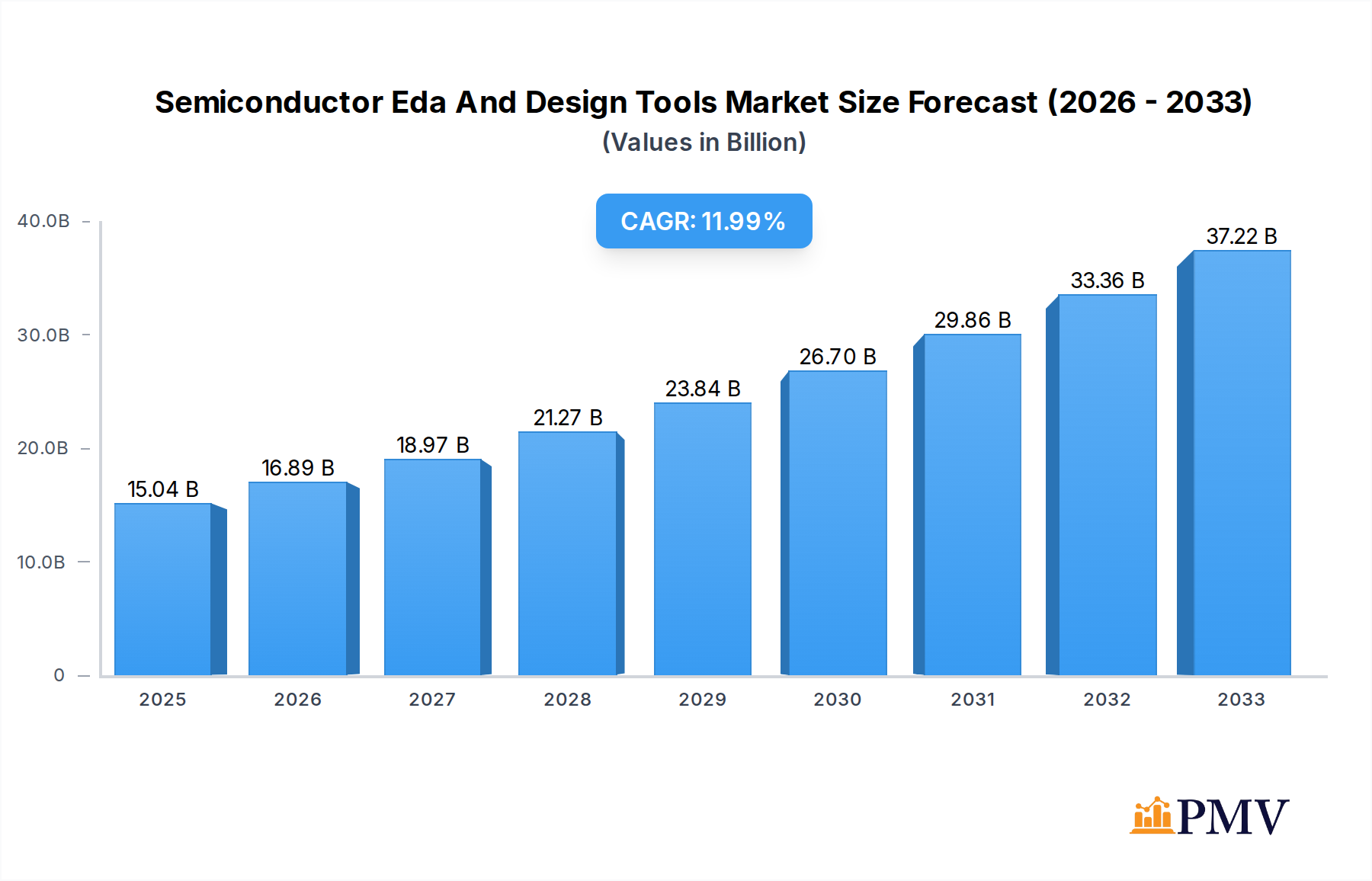
The global Semiconductor EDA and Design Tools market is poised for robust expansion, with an estimated market size of $15,038.7 million in 2025 and a projected CAGR of 12.3% from 2019 to 2033. This significant growth is fueled by the escalating demand for advanced semiconductor chips across a multitude of industries. The automotive sector is a primary driver, with the increasing adoption of sophisticated electronic systems for autonomous driving, infotainment, and electric vehicle power management. Similarly, the consumer electronics market continues to innovate, necessitating more complex and powerful chip designs for smartphones, wearables, and smart home devices. Industrial automation and the expansion of 5G communication networks are also significant contributors, creating a continuous need for optimized and high-performance integrated circuits (ICs). The medical sector's reliance on miniaturized and reliable semiconductor components for advanced diagnostic and therapeutic devices further bolsters this demand.

Semiconductor Eda And Design Tools Market Size (In Billion)
Key trends shaping the market include the rise of AI and machine learning integration within EDA tools themselves, enhancing design efficiency and predictive capabilities. The increasing complexity of IC design, with a growing number of transistors and intricate architectures, is driving the adoption of advanced Electronic Circuit Design and Simulation and PCB Design solutions. Furthermore, the geopolitical landscape and supply chain considerations are subtly influencing regional investments and tool development. While the market benefits from strong demand, it faces potential restraints such as the high cost of advanced EDA software and the shortage of skilled design engineers. Nevertheless, the industry is characterized by intense competition among major players like Cadence, Synopsys, and Siemens, all striving to offer cutting-edge solutions that meet the evolving needs of chip manufacturers globally. The market's trajectory indicates a sustained period of innovation and growth, driven by the relentless pursuit of smaller, faster, and more power-efficient semiconductor devices.
Semiconductor Eda And Design Tools Company Market Share
Semiconductor EDA and Design Tools Market: Comprehensive Analysis and Future Outlook
This in-depth report provides a detailed market analysis of Semiconductor Electronic Design Automation (EDA) and Design Tools, offering critical insights into market structure, competitive dynamics, industry trends, dominant segments, product innovations, and future strategic outlook. Covering a study period from 2019–2033, with a base year of 2025 and a forecast period of 2025–2033, this report is an indispensable resource for stakeholders seeking to understand and capitalize on the evolving landscape of semiconductor design. We meticulously analyze key players, market drivers, challenges, and segmentation across crucial application and type categories, providing actionable intelligence for strategic decision-making.
Semiconductor Eda And Design Tools Market Structure & Competitive Dynamics
The global Semiconductor EDA and Design Tools market exhibits a moderately concentrated structure, dominated by a few key players who command significant market share. Major companies like Cadence Design Systems, Synopsys, and Siemens Digital Industries Software hold substantial portions of the market, driven by their comprehensive portfolios of advanced EDA solutions. Innovation ecosystems are robust, fueled by continuous research and development in areas like AI-driven design, advanced node enablement, and multi-physics simulation. Regulatory frameworks, while generally permissive, focus on intellectual property protection and trade compliance. Product substitutes are limited, primarily comprising in-house developed tools or less sophisticated open-source alternatives, which often lack the breadth and depth of commercial offerings. End-user trends highlight an increasing demand for specialized EDA tools catering to emerging applications in automotive electronics, high-performance computing, and artificial intelligence. Mergers and Acquisition (M&A) activities are strategic, aimed at consolidating market presence, acquiring complementary technologies, or expanding into new market segments. Recent M&A deal values are estimated in the range of hundreds of million to billions of dollars, reflecting the strategic importance of these acquisitions. The competitive landscape is characterized by intense innovation, strategic partnerships, and a focus on providing integrated design flows to address the complexity of modern chip development.
Semiconductor Eda And Design Tools Industry Trends & Insights
The Semiconductor EDA and Design Tools industry is experiencing robust growth, driven by an insatiable demand for increasingly sophisticated and powerful electronic devices. The Compound Annual Growth Rate (CAGR) for this market is projected to be in the high single digits throughout the forecast period. Key market growth drivers include the exponential rise of data generation and processing, necessitating advanced semiconductor chips. The proliferation of the Internet of Things (IoT), 5G communication, artificial intelligence (AI) and machine learning (ML) applications, and the ever-expanding automotive sector, particularly electric and autonomous vehicles, are fundamentally reshaping the demand for specialized chip designs and, consequently, EDA tools. Technological disruptions are continuously redefining the capabilities of EDA software. These include the integration of AI and ML for optimizing design processes, reducing design cycles, and enhancing verification efficiency. Advancements in cloud-based EDA solutions are also gaining traction, offering scalability, accessibility, and collaborative design capabilities to a wider user base. Furthermore, the increasing complexity of semiconductor manufacturing processes, particularly at advanced nodes (e.g., 5nm, 3nm, and below), demands highly accurate and sophisticated simulation and verification tools to ensure design integrity and yield. Consumer preferences are increasingly dictating the need for smaller, more power-efficient, and higher-performance devices, pushing semiconductor manufacturers to innovate rapidly. This, in turn, drives the demand for EDA tools that can facilitate such innovations. Competitive dynamics are fierce, with major players investing heavily in R&D to maintain their technological edge. The market penetration of advanced EDA solutions is steadily increasing as the benefits of these tools in accelerating time-to-market and reducing development costs become more apparent. The ongoing trend towards heterogeneous integration and advanced packaging techniques also presents new challenges and opportunities for EDA vendors, requiring novel solutions for multi-chip design and co-simulation. The report estimates the total market size to reach tens of billions of dollars by the end of the forecast period.
Dominant Markets & Segments in Semiconductor Eda And Design Tools
The Semiconductor EDA and Design Tools market is characterized by strong regional and segment-specific dominance, driven by a confluence of economic policies, technological infrastructure, and industry adoption rates. Geographically, North America and Asia-Pacific are emerging as dominant markets. In North America, significant investment in R&D for AI, high-performance computing, and advanced defense applications fuels demand for sophisticated EDA solutions. Favorable economic policies, a strong presence of semiconductor R&D centers, and a highly skilled workforce contribute to its leadership. Asia-Pacific, particularly countries like Taiwan, South Korea, and China, holds a substantial market share due to its extensive semiconductor manufacturing capabilities and its role as a global hub for electronics production. Government initiatives supporting domestic semiconductor development and the massive consumer electronics market further bolster demand.
Key Drivers of Dominance:
- Economic Policies: Government incentives, R&D tax credits, and strategic investments in the semiconductor industry.
- Infrastructure: Robust semiconductor manufacturing facilities, advanced research institutions, and well-developed logistics networks.
- End-User Demand: High consumer demand for electronics, rapid adoption of new technologies, and significant investments in emerging sectors.
Dominance Analysis by Segment:
Application Segments:
- Automotive: This segment is experiencing rapid growth, driven by the electrification of vehicles, the development of advanced driver-assistance systems (ADAS), and the increasing adoption of in-car infotainment and connectivity features. EDA tools are crucial for designing complex automotive-grade microcontrollers, sensors, and communication chips. The market size for automotive EDA tools is projected to exceed several billion dollars within the forecast period.
- Consumer Electronics: Remains a significant market, propelled by the continuous demand for smartphones, wearables, smart home devices, and gaming consoles. EDA tools are essential for optimizing power efficiency, performance, and miniaturization of chips in these devices. This segment represents a substantial portion of the overall market value, likely in the tens of billions.
- Communication: Driven by the rollout of 5G networks, the development of advanced communication chips for infrastructure and user devices, and the expansion of IoT connectivity. EDA solutions are vital for designing high-frequency components, complex signal processing units, and robust network interface controllers. The market size is estimated to be in the billions.
- Industrial: Growing demand for automation, robotics, and smart manufacturing, coupled with the increasing use of IoT in industrial settings, fuels the need for specialized industrial control chips, sensors, and power management ICs. EDA tools play a critical role in designing reliable and efficient industrial-grade semiconductors. The market size is projected to be in the billions.
- Aerospace and Defense: This segment requires highly reliable, high-performance, and often custom-designed chips for critical applications such as radar systems, navigation, satellite communication, and advanced weaponry. EDA tools with advanced verification capabilities and support for stringent reliability standards are in high demand. While smaller in volume than consumer electronics, it represents a high-value market, estimated in the hundreds of millions.
- Medical: Driven by advancements in medical imaging, portable diagnostic devices, implantable electronics, and personalized medicine, this segment demands highly accurate and reliable semiconductor components. EDA tools are crucial for designing specialized ICs for medical devices. The market size is in the hundreds of millions.
- Others: This encompasses emerging applications and niche markets, contributing to overall market growth.
Type Segments:
- IC Design: This is the largest and most critical segment, encompassing the entire process of designing integrated circuits, from conceptualization to physical implementation. EDA tools for logic synthesis, place and route, physical verification, and analog/mixed-signal design are paramount. The market size is expected to dominate, likely exceeding tens of billions of dollars.
- Electronic Circuit Design and Simulation: This segment includes tools for simulating and analyzing electronic circuits at various levels of abstraction, crucial for verifying functionality and performance before committing to physical design. It is a foundational element supporting IC design and PCB design. The market size is estimated to be in the billions.
- PCB Design: Focuses on the layout and routing of printed circuit boards, integrating various components. With the increasing complexity of modern electronic systems, advanced PCB design tools are essential for managing signal integrity, power delivery, and thermal management. The market size is estimated to be in the billions.
Semiconductor Eda And Design Tools Product Innovations
Product innovations in Semiconductor EDA and Design Tools are rapidly advancing, driven by the need for enhanced performance, reduced power consumption, and accelerated design cycles. Key developments include the integration of Artificial Intelligence (AI) and Machine Learning (ML) into EDA workflows for automated design exploration, optimization, and verification, leading to significant time-to-market reductions. Cloud-native EDA platforms are emerging, offering scalable computing resources and collaborative design environments. Furthermore, advancements in multi-physics simulation tools are enabling more accurate modeling of complex physical phenomena, critical for advanced node designs and specialized applications. Competitive advantages are being gained by vendors offering integrated design flows that seamlessly connect different stages of the chip development process, from RTL to GDSII, and support heterogeneous integration and advanced packaging.
Report Segmentation & Scope
This report meticulously segments the Semiconductor EDA and Design Tools market across key parameters to provide a granular understanding of its dynamics.
- Application Segmentation: The market is segmented into Automotive, Industrial, Consumer Electronics, Communication, Medical, Aerospace and Defense, and Others. Each segment is analyzed for its specific demand drivers, growth projections, market sizes, and competitive dynamics within the broader EDA landscape. The Automotive and Consumer Electronics segments are expected to exhibit the highest growth rates and market penetration.
- Type Segmentation: The report further categorizes the market by Type, including Electronic Circuit Design and Simulation, PCB Design, and IC Design. IC Design represents the largest segment due to its foundational role in chip development, followed by PCB Design and Electronic Circuit Design and Simulation, all of which are crucial enablers of innovation. Growth projections and competitive landscapes are detailed for each type.
Key Drivers of Semiconductor Eda And Design Tools Growth
The growth of the Semiconductor EDA and Design Tools market is propelled by several interconnected factors. The relentless pursuit of higher performance and increased functionality in electronic devices, fueled by advancements in AI, 5G, IoT, and autonomous systems, directly translates to a demand for more sophisticated semiconductor chips and, consequently, advanced EDA tools. Technological advancements, such as the push towards smaller process nodes (e.g., 3nm and below), necessitate highly accurate and complex simulation and verification capabilities offered by leading EDA solutions. Economic growth and increasing disposable incomes in emerging economies are driving consumer demand for electronics, further stimulating the semiconductor industry. Regulatory drivers, such as the increasing emphasis on cybersecurity and data privacy, also influence chip design requirements, indirectly impacting the EDA market. Strategic investments by governments in domestic semiconductor manufacturing capabilities and R&D initiatives globally are also significant growth accelerators.
Challenges in the Semiconductor Eda And Design Tools Sector
Despite its robust growth, the Semiconductor EDA and Design Tools sector faces several challenges. The increasing complexity of chip designs, particularly at advanced process nodes, leads to escalating tool development and verification costs for EDA vendors. High upfront investment and long development cycles for cutting-edge EDA tools can be a barrier to entry for smaller players. The shortage of skilled EDA engineers and chip designers, a global challenge, can hinder the adoption and effective utilization of advanced tools. Supply chain disruptions, as witnessed in recent years, can impact the availability of essential hardware components required for semiconductor manufacturing, indirectly affecting demand for EDA tools. Intense competition among EDA vendors leads to price pressures and the need for continuous innovation to maintain market share. Furthermore, the evolving regulatory landscape concerning intellectual property and international trade can create uncertainties and compliance burdens. The sheer scale of data generated during complex chip design and verification also presents significant computational and storage challenges.
Leading Players in the Semiconductor Eda And Design Tools Market
- Cadence Design Systems
- Synopsys
- Siemens Digital Industries Software
- Ansys
- Silvaco
- Keysight Technologies
- Aldec
- Primarius Technologies
- Empyrean Technology
Key Developments in Semiconductor Eda And Design Tools Sector
- 2023/08: Cadence announces a new suite of AI-driven EDA tools for chip design, aiming to accelerate verification cycles and improve design closure.
- 2023/05: Synopsys launches its next-generation chip design platform, enhancing support for multi-chip packaging and advanced node technologies.
- 2023/02: Siemens Digital Industries Software expands its Xcelerator portfolio with new capabilities for system-level design and embedded software co-development.
- 2022/11: Ansys introduces advanced simulation solutions for next-generation power electronics, crucial for electric vehicle and renewable energy applications.
- 2022/07: Silvaco releases new SPICE simulation models for emerging semiconductor technologies, supporting innovation in advanced materials.
- 2022/04: Keysight Technologies announces a collaboration with a leading foundry to optimize test solutions for advanced semiconductor nodes.
- 2021/12: Aldec introduces a new simulation engine for FPGA design, offering enhanced performance and broader device support.
- 2021/09: Primarius Technologies unveils its latest parasitic extraction tool, crucial for ensuring signal integrity in high-speed designs.
- 2021/06: Empyrean Technology announces significant upgrades to its IC layout and verification suite, targeting complex analog and mixed-signal designs.
Strategic Semiconductor Eda And Design Tools Market Outlook
The strategic outlook for the Semiconductor EDA and Design Tools market remains exceptionally strong, driven by the foundational role these tools play in enabling technological advancement across virtually all industries. Growth accelerators include the burgeoning demand for AI-optimized chips, the pervasive expansion of IoT devices, and the rapid evolution of communication technologies. The increasing complexity of semiconductor architectures, including multi-chip modules and advanced packaging, will continue to fuel demand for sophisticated EDA solutions. Strategic opportunities lie in developing AI-native EDA tools that can automate complex design tasks, offering significant time and cost savings to chip manufacturers. The expansion of cloud-based EDA services presents a significant avenue for growth, enabling greater accessibility and scalability. Furthermore, vendors who can provide comprehensive, integrated design flows that address the entire semiconductor lifecycle, from concept to manufacturing and testing, will be best positioned for success. The ongoing investment in domestic semiconductor ecosystems globally also presents a significant market expansion potential.
Semiconductor Eda And Design Tools Segmentation
-
1. Application
- 1.1. Automotive
- 1.2. Industrial
- 1.3. Consumer Electronics
- 1.4. Communication
- 1.5. Medical
- 1.6. Aerospace and Defense
- 1.7. Others
-
2. Type
- 2.1. Electronic Circuit Design and Simulation
- 2.2. PCB Design
- 2.3. IC Design
Semiconductor Eda And Design Tools Segmentation By Geography
-
1. North America
- 1.1. United States
- 1.2. Canada
- 1.3. Mexico
-
2. South America
- 2.1. Brazil
- 2.2. Argentina
- 2.3. Rest of South America
-
3. Europe
- 3.1. United Kingdom
- 3.2. Germany
- 3.3. France
- 3.4. Italy
- 3.5. Spain
- 3.6. Russia
- 3.7. Benelux
- 3.8. Nordics
- 3.9. Rest of Europe
-
4. Middle East & Africa
- 4.1. Turkey
- 4.2. Israel
- 4.3. GCC
- 4.4. North Africa
- 4.5. South Africa
- 4.6. Rest of Middle East & Africa
-
5. Asia Pacific
- 5.1. China
- 5.2. India
- 5.3. Japan
- 5.4. South Korea
- 5.5. ASEAN
- 5.6. Oceania
- 5.7. Rest of Asia Pacific
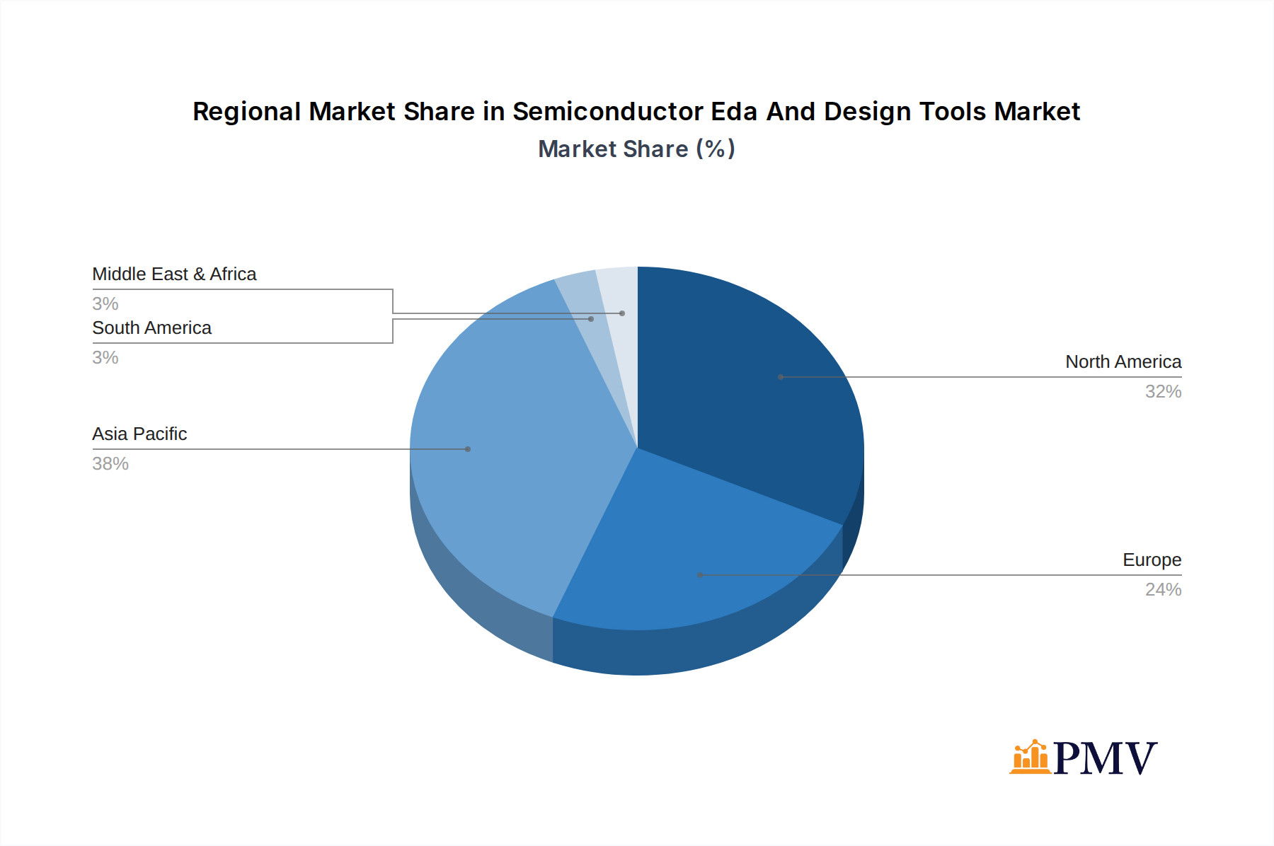
Semiconductor Eda And Design Tools Regional Market Share
Geographic Coverage of Semiconductor Eda And Design Tools
Semiconductor Eda And Design Tools REPORT HIGHLIGHTS
| Aspects | Details |
|---|---|
| Study Period | 2020-2034 |
| Base Year | 2025 |
| Estimated Year | 2026 |
| Forecast Period | 2026-2034 |
| Historical Period | 2020-2025 |
| Growth Rate | CAGR of 12.3% from 2020-2034 |
| Segmentation |
|
Table of Contents
- 1. Introduction
- 1.1. Research Scope
- 1.2. Market Segmentation
- 1.3. Research Objective
- 1.4. Definitions and Assumptions
- 2. Executive Summary
- 2.1. Market Snapshot
- 3. Market Dynamics
- 3.1. Market Drivers
- 3.2. Market Restrains
- 3.3. Market Trends
- 3.4. Market Opportunities
- 4. Market Factor Analysis
- 4.1. Porters Five Forces
- 4.1.1. Bargaining Power of Suppliers
- 4.1.2. Bargaining Power of Buyers
- 4.1.3. Threat of New Entrants
- 4.1.4. Threat of Substitutes
- 4.1.5. Competitive Rivalry
- 4.2. PESTEL analysis
- 4.3. BCG Analysis
- 4.3.1. Stars (High Growth, High Market Share)
- 4.3.2. Cash Cows (Low Growth, High Market Share)
- 4.3.3. Question Mark (High Growth, Low Market Share)
- 4.3.4. Dogs (Low Growth, Low Market Share)
- 4.4. Ansoff Matrix Analysis
- 4.5. Supply Chain Analysis
- 4.6. Regulatory Landscape
- 4.7. Current Market Potential and Opportunity Assessment (TAM–SAM–SOM Framework)
- 4.8. PMV Analyst Note
- 4.1. Porters Five Forces
- 5. Market Analysis, Insights and Forecast 2021-2033
- 5.1. Market Analysis, Insights and Forecast - by Application
- 5.1.1. Automotive
- 5.1.2. Industrial
- 5.1.3. Consumer Electronics
- 5.1.4. Communication
- 5.1.5. Medical
- 5.1.6. Aerospace and Defense
- 5.1.7. Others
- 5.2. Market Analysis, Insights and Forecast - by Type
- 5.2.1. Electronic Circuit Design and Simulation
- 5.2.2. PCB Design
- 5.2.3. IC Design
- 5.3. Market Analysis, Insights and Forecast - by Region
- 5.3.1. North America
- 5.3.2. South America
- 5.3.3. Europe
- 5.3.4. Middle East & Africa
- 5.3.5. Asia Pacific
- 5.1. Market Analysis, Insights and Forecast - by Application
- 6. Global Semiconductor Eda And Design Tools Analysis, Insights and Forecast, 2021-2033
- 6.1. Market Analysis, Insights and Forecast - by Application
- 6.1.1. Automotive
- 6.1.2. Industrial
- 6.1.3. Consumer Electronics
- 6.1.4. Communication
- 6.1.5. Medical
- 6.1.6. Aerospace and Defense
- 6.1.7. Others
- 6.2. Market Analysis, Insights and Forecast - by Type
- 6.2.1. Electronic Circuit Design and Simulation
- 6.2.2. PCB Design
- 6.2.3. IC Design
- 6.1. Market Analysis, Insights and Forecast - by Application
- 7. North America Semiconductor Eda And Design Tools Analysis, Insights and Forecast, 2020-2032
- 7.1. Market Analysis, Insights and Forecast - by Application
- 7.1.1. Automotive
- 7.1.2. Industrial
- 7.1.3. Consumer Electronics
- 7.1.4. Communication
- 7.1.5. Medical
- 7.1.6. Aerospace and Defense
- 7.1.7. Others
- 7.2. Market Analysis, Insights and Forecast - by Type
- 7.2.1. Electronic Circuit Design and Simulation
- 7.2.2. PCB Design
- 7.2.3. IC Design
- 7.1. Market Analysis, Insights and Forecast - by Application
- 8. South America Semiconductor Eda And Design Tools Analysis, Insights and Forecast, 2020-2032
- 8.1. Market Analysis, Insights and Forecast - by Application
- 8.1.1. Automotive
- 8.1.2. Industrial
- 8.1.3. Consumer Electronics
- 8.1.4. Communication
- 8.1.5. Medical
- 8.1.6. Aerospace and Defense
- 8.1.7. Others
- 8.2. Market Analysis, Insights and Forecast - by Type
- 8.2.1. Electronic Circuit Design and Simulation
- 8.2.2. PCB Design
- 8.2.3. IC Design
- 8.1. Market Analysis, Insights and Forecast - by Application
- 9. Europe Semiconductor Eda And Design Tools Analysis, Insights and Forecast, 2020-2032
- 9.1. Market Analysis, Insights and Forecast - by Application
- 9.1.1. Automotive
- 9.1.2. Industrial
- 9.1.3. Consumer Electronics
- 9.1.4. Communication
- 9.1.5. Medical
- 9.1.6. Aerospace and Defense
- 9.1.7. Others
- 9.2. Market Analysis, Insights and Forecast - by Type
- 9.2.1. Electronic Circuit Design and Simulation
- 9.2.2. PCB Design
- 9.2.3. IC Design
- 9.1. Market Analysis, Insights and Forecast - by Application
- 10. Middle East & Africa Semiconductor Eda And Design Tools Analysis, Insights and Forecast, 2020-2032
- 10.1. Market Analysis, Insights and Forecast - by Application
- 10.1.1. Automotive
- 10.1.2. Industrial
- 10.1.3. Consumer Electronics
- 10.1.4. Communication
- 10.1.5. Medical
- 10.1.6. Aerospace and Defense
- 10.1.7. Others
- 10.2. Market Analysis, Insights and Forecast - by Type
- 10.2.1. Electronic Circuit Design and Simulation
- 10.2.2. PCB Design
- 10.2.3. IC Design
- 10.1. Market Analysis, Insights and Forecast - by Application
- 11. Asia Pacific Semiconductor Eda And Design Tools Analysis, Insights and Forecast, 2020-2032
- 11.1. Market Analysis, Insights and Forecast - by Application
- 11.1.1. Automotive
- 11.1.2. Industrial
- 11.1.3. Consumer Electronics
- 11.1.4. Communication
- 11.1.5. Medical
- 11.1.6. Aerospace and Defense
- 11.1.7. Others
- 11.2. Market Analysis, Insights and Forecast - by Type
- 11.2.1. Electronic Circuit Design and Simulation
- 11.2.2. PCB Design
- 11.2.3. IC Design
- 11.1. Market Analysis, Insights and Forecast - by Application
- 12. Competitive Analysis
- 12.1. Company Profiles
- 12.1.1 Cadence
- 12.1.1.1. Company Overview
- 12.1.1.2. Products
- 12.1.1.3. Company Financials
- 12.1.1.4. SWOT Analysis
- 12.1.2 Synopsys
- 12.1.2.1. Company Overview
- 12.1.2.2. Products
- 12.1.2.3. Company Financials
- 12.1.2.4. SWOT Analysis
- 12.1.3 Siemens
- 12.1.3.1. Company Overview
- 12.1.3.2. Products
- 12.1.3.3. Company Financials
- 12.1.3.4. SWOT Analysis
- 12.1.4 Ansys
- 12.1.4.1. Company Overview
- 12.1.4.2. Products
- 12.1.4.3. Company Financials
- 12.1.4.4. SWOT Analysis
- 12.1.5 Silvaco
- 12.1.5.1. Company Overview
- 12.1.5.2. Products
- 12.1.5.3. Company Financials
- 12.1.5.4. SWOT Analysis
- 12.1.6 Keysight Technologies
- 12.1.6.1. Company Overview
- 12.1.6.2. Products
- 12.1.6.3. Company Financials
- 12.1.6.4. SWOT Analysis
- 12.1.7 Aldec
- 12.1.7.1. Company Overview
- 12.1.7.2. Products
- 12.1.7.3. Company Financials
- 12.1.7.4. SWOT Analysis
- 12.1.8 Primarius Technologies
- 12.1.8.1. Company Overview
- 12.1.8.2. Products
- 12.1.8.3. Company Financials
- 12.1.8.4. SWOT Analysis
- 12.1.9 Empyrean Technology
- 12.1.9.1. Company Overview
- 12.1.9.2. Products
- 12.1.9.3. Company Financials
- 12.1.9.4. SWOT Analysis
- 12.1.1 Cadence
- 12.2. Market Entropy
- 12.2.1 Company's Key Areas Served
- 12.2.2 Recent Developments
- 12.3. Company Market Share Analysis 2025
- 12.3.1 Top 5 Companies Market Share Analysis
- 12.3.2 Top 3 Companies Market Share Analysis
- 12.4. List of Potential Customers
- 13. Research Methodology
List of Figures
- Figure 1: Global Semiconductor Eda And Design Tools Revenue Breakdown (undefined, %) by Region 2025 & 2033
- Figure 2: North America Semiconductor Eda And Design Tools Revenue (undefined), by Application 2025 & 2033
- Figure 3: North America Semiconductor Eda And Design Tools Revenue Share (%), by Application 2025 & 2033
- Figure 4: North America Semiconductor Eda And Design Tools Revenue (undefined), by Type 2025 & 2033
- Figure 5: North America Semiconductor Eda And Design Tools Revenue Share (%), by Type 2025 & 2033
- Figure 6: North America Semiconductor Eda And Design Tools Revenue (undefined), by Country 2025 & 2033
- Figure 7: North America Semiconductor Eda And Design Tools Revenue Share (%), by Country 2025 & 2033
- Figure 8: South America Semiconductor Eda And Design Tools Revenue (undefined), by Application 2025 & 2033
- Figure 9: South America Semiconductor Eda And Design Tools Revenue Share (%), by Application 2025 & 2033
- Figure 10: South America Semiconductor Eda And Design Tools Revenue (undefined), by Type 2025 & 2033
- Figure 11: South America Semiconductor Eda And Design Tools Revenue Share (%), by Type 2025 & 2033
- Figure 12: South America Semiconductor Eda And Design Tools Revenue (undefined), by Country 2025 & 2033
- Figure 13: South America Semiconductor Eda And Design Tools Revenue Share (%), by Country 2025 & 2033
- Figure 14: Europe Semiconductor Eda And Design Tools Revenue (undefined), by Application 2025 & 2033
- Figure 15: Europe Semiconductor Eda And Design Tools Revenue Share (%), by Application 2025 & 2033
- Figure 16: Europe Semiconductor Eda And Design Tools Revenue (undefined), by Type 2025 & 2033
- Figure 17: Europe Semiconductor Eda And Design Tools Revenue Share (%), by Type 2025 & 2033
- Figure 18: Europe Semiconductor Eda And Design Tools Revenue (undefined), by Country 2025 & 2033
- Figure 19: Europe Semiconductor Eda And Design Tools Revenue Share (%), by Country 2025 & 2033
- Figure 20: Middle East & Africa Semiconductor Eda And Design Tools Revenue (undefined), by Application 2025 & 2033
- Figure 21: Middle East & Africa Semiconductor Eda And Design Tools Revenue Share (%), by Application 2025 & 2033
- Figure 22: Middle East & Africa Semiconductor Eda And Design Tools Revenue (undefined), by Type 2025 & 2033
- Figure 23: Middle East & Africa Semiconductor Eda And Design Tools Revenue Share (%), by Type 2025 & 2033
- Figure 24: Middle East & Africa Semiconductor Eda And Design Tools Revenue (undefined), by Country 2025 & 2033
- Figure 25: Middle East & Africa Semiconductor Eda And Design Tools Revenue Share (%), by Country 2025 & 2033
- Figure 26: Asia Pacific Semiconductor Eda And Design Tools Revenue (undefined), by Application 2025 & 2033
- Figure 27: Asia Pacific Semiconductor Eda And Design Tools Revenue Share (%), by Application 2025 & 2033
- Figure 28: Asia Pacific Semiconductor Eda And Design Tools Revenue (undefined), by Type 2025 & 2033
- Figure 29: Asia Pacific Semiconductor Eda And Design Tools Revenue Share (%), by Type 2025 & 2033
- Figure 30: Asia Pacific Semiconductor Eda And Design Tools Revenue (undefined), by Country 2025 & 2033
- Figure 31: Asia Pacific Semiconductor Eda And Design Tools Revenue Share (%), by Country 2025 & 2033
List of Tables
- Table 1: Global Semiconductor Eda And Design Tools Revenue undefined Forecast, by Application 2020 & 2033
- Table 2: Global Semiconductor Eda And Design Tools Revenue undefined Forecast, by Type 2020 & 2033
- Table 3: Global Semiconductor Eda And Design Tools Revenue undefined Forecast, by Region 2020 & 2033
- Table 4: Global Semiconductor Eda And Design Tools Revenue undefined Forecast, by Application 2020 & 2033
- Table 5: Global Semiconductor Eda And Design Tools Revenue undefined Forecast, by Type 2020 & 2033
- Table 6: Global Semiconductor Eda And Design Tools Revenue undefined Forecast, by Country 2020 & 2033
- Table 7: United States Semiconductor Eda And Design Tools Revenue (undefined) Forecast, by Application 2020 & 2033
- Table 8: Canada Semiconductor Eda And Design Tools Revenue (undefined) Forecast, by Application 2020 & 2033
- Table 9: Mexico Semiconductor Eda And Design Tools Revenue (undefined) Forecast, by Application 2020 & 2033
- Table 10: Global Semiconductor Eda And Design Tools Revenue undefined Forecast, by Application 2020 & 2033
- Table 11: Global Semiconductor Eda And Design Tools Revenue undefined Forecast, by Type 2020 & 2033
- Table 12: Global Semiconductor Eda And Design Tools Revenue undefined Forecast, by Country 2020 & 2033
- Table 13: Brazil Semiconductor Eda And Design Tools Revenue (undefined) Forecast, by Application 2020 & 2033
- Table 14: Argentina Semiconductor Eda And Design Tools Revenue (undefined) Forecast, by Application 2020 & 2033
- Table 15: Rest of South America Semiconductor Eda And Design Tools Revenue (undefined) Forecast, by Application 2020 & 2033
- Table 16: Global Semiconductor Eda And Design Tools Revenue undefined Forecast, by Application 2020 & 2033
- Table 17: Global Semiconductor Eda And Design Tools Revenue undefined Forecast, by Type 2020 & 2033
- Table 18: Global Semiconductor Eda And Design Tools Revenue undefined Forecast, by Country 2020 & 2033
- Table 19: United Kingdom Semiconductor Eda And Design Tools Revenue (undefined) Forecast, by Application 2020 & 2033
- Table 20: Germany Semiconductor Eda And Design Tools Revenue (undefined) Forecast, by Application 2020 & 2033
- Table 21: France Semiconductor Eda And Design Tools Revenue (undefined) Forecast, by Application 2020 & 2033
- Table 22: Italy Semiconductor Eda And Design Tools Revenue (undefined) Forecast, by Application 2020 & 2033
- Table 23: Spain Semiconductor Eda And Design Tools Revenue (undefined) Forecast, by Application 2020 & 2033
- Table 24: Russia Semiconductor Eda And Design Tools Revenue (undefined) Forecast, by Application 2020 & 2033
- Table 25: Benelux Semiconductor Eda And Design Tools Revenue (undefined) Forecast, by Application 2020 & 2033
- Table 26: Nordics Semiconductor Eda And Design Tools Revenue (undefined) Forecast, by Application 2020 & 2033
- Table 27: Rest of Europe Semiconductor Eda And Design Tools Revenue (undefined) Forecast, by Application 2020 & 2033
- Table 28: Global Semiconductor Eda And Design Tools Revenue undefined Forecast, by Application 2020 & 2033
- Table 29: Global Semiconductor Eda And Design Tools Revenue undefined Forecast, by Type 2020 & 2033
- Table 30: Global Semiconductor Eda And Design Tools Revenue undefined Forecast, by Country 2020 & 2033
- Table 31: Turkey Semiconductor Eda And Design Tools Revenue (undefined) Forecast, by Application 2020 & 2033
- Table 32: Israel Semiconductor Eda And Design Tools Revenue (undefined) Forecast, by Application 2020 & 2033
- Table 33: GCC Semiconductor Eda And Design Tools Revenue (undefined) Forecast, by Application 2020 & 2033
- Table 34: North Africa Semiconductor Eda And Design Tools Revenue (undefined) Forecast, by Application 2020 & 2033
- Table 35: South Africa Semiconductor Eda And Design Tools Revenue (undefined) Forecast, by Application 2020 & 2033
- Table 36: Rest of Middle East & Africa Semiconductor Eda And Design Tools Revenue (undefined) Forecast, by Application 2020 & 2033
- Table 37: Global Semiconductor Eda And Design Tools Revenue undefined Forecast, by Application 2020 & 2033
- Table 38: Global Semiconductor Eda And Design Tools Revenue undefined Forecast, by Type 2020 & 2033
- Table 39: Global Semiconductor Eda And Design Tools Revenue undefined Forecast, by Country 2020 & 2033
- Table 40: China Semiconductor Eda And Design Tools Revenue (undefined) Forecast, by Application 2020 & 2033
- Table 41: India Semiconductor Eda And Design Tools Revenue (undefined) Forecast, by Application 2020 & 2033
- Table 42: Japan Semiconductor Eda And Design Tools Revenue (undefined) Forecast, by Application 2020 & 2033
- Table 43: South Korea Semiconductor Eda And Design Tools Revenue (undefined) Forecast, by Application 2020 & 2033
- Table 44: ASEAN Semiconductor Eda And Design Tools Revenue (undefined) Forecast, by Application 2020 & 2033
- Table 45: Oceania Semiconductor Eda And Design Tools Revenue (undefined) Forecast, by Application 2020 & 2033
- Table 46: Rest of Asia Pacific Semiconductor Eda And Design Tools Revenue (undefined) Forecast, by Application 2020 & 2033
Frequently Asked Questions
1. What is the projected Compound Annual Growth Rate (CAGR) of the Semiconductor Eda And Design Tools?
The projected CAGR is approximately 12.3%.
2. Which companies are prominent players in the Semiconductor Eda And Design Tools?
Key companies in the market include Cadence, Synopsys, Siemens, Ansys, Silvaco, Keysight Technologies, Aldec, Primarius Technologies, Empyrean Technology.
3. What are the main segments of the Semiconductor Eda And Design Tools?
The market segments include Application, Type.
4. Can you provide details about the market size?
The market size is estimated to be USD XXX N/A as of 2022.
5. What are some drivers contributing to market growth?
N/A
6. What are the notable trends driving market growth?
N/A
7. Are there any restraints impacting market growth?
N/A
8. Can you provide examples of recent developments in the market?
N/A
9. What pricing options are available for accessing the report?
Pricing options include single-user, multi-user, and enterprise licenses priced at USD 2900.00, USD 4350.00, and USD 5800.00 respectively.
10. Is the market size provided in terms of value or volume?
The market size is provided in terms of value, measured in N/A.
11. Are there any specific market keywords associated with the report?
Yes, the market keyword associated with the report is "Semiconductor Eda And Design Tools," which aids in identifying and referencing the specific market segment covered.
12. How do I determine which pricing option suits my needs best?
The pricing options vary based on user requirements and access needs. Individual users may opt for single-user licenses, while businesses requiring broader access may choose multi-user or enterprise licenses for cost-effective access to the report.
13. Are there any additional resources or data provided in the Semiconductor Eda And Design Tools report?
While the report offers comprehensive insights, it's advisable to review the specific contents or supplementary materials provided to ascertain if additional resources or data are available.
14. How can I stay updated on further developments or reports in the Semiconductor Eda And Design Tools?
To stay informed about further developments, trends, and reports in the Semiconductor Eda And Design Tools, consider subscribing to industry newsletters, following relevant companies and organizations, or regularly checking reputable industry news sources and publications.
Methodology
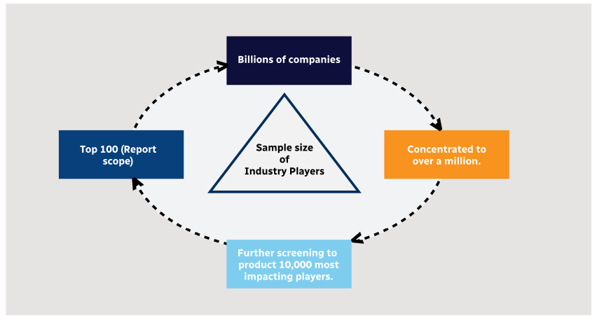
Step 1 - Identification of Relevant Samples Size from Population Database

Step 2 - Approaches for Defining Global Market Size (Value, Volume* & Price*)
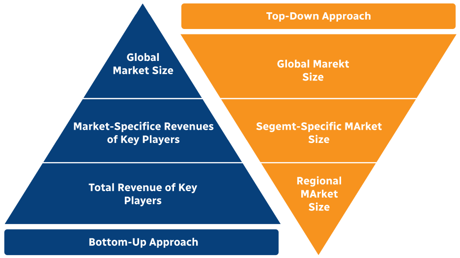
Note*: In applicable scenarios
Step 3 - Data Sources
Primary Research
- Web Analytics
- Survey Reports
- Research Institute
- Latest Research Reports
- Opinion Leaders
Secondary Research
- Annual Reports
- White Paper
- Latest Press Release
- Industry Association
- Paid Database
- Investor Presentations

Step 4 - Data Triangulation
Involves using different sources of information in order to increase the validity of a study
These sources are likely to be stakeholders in a program - participants, other researchers, program staff, other community members, and so on.
Then we put all data in single framework & apply various statistical tools to find out the dynamic on the market.
During the analysis stage, feedback from the stakeholder groups would be compared to determine areas of agreement as well as areas of divergence