


Key Insights
The global Semiconductor Optical Measurement Equipment market is poised for significant expansion, projected to reach USD 14.92 billion in 2025. This robust growth is fueled by the relentless pursuit of miniaturization and increased complexity in semiconductor manufacturing. As wafer features shrink and device performance demands escalate, the precision and accuracy offered by optical measurement techniques become indispensable. Key drivers include the burgeoning demand for advanced semiconductors in consumer electronics, automotive, AI, and 5G infrastructure, all of which necessitate highly sophisticated inspection and metrology solutions. The increasing prevalence of complex chip architectures, such as 3D NAND and advanced logic devices, further amplifies the need for precise measurement of critical dimensions, overlay accuracy, and film thickness. The market is experiencing a healthy CAGR of 6.9%, indicating sustained momentum and a strong outlook for the coming years, with the forecast period from 2025 to 2033 expected to witness substantial value creation.
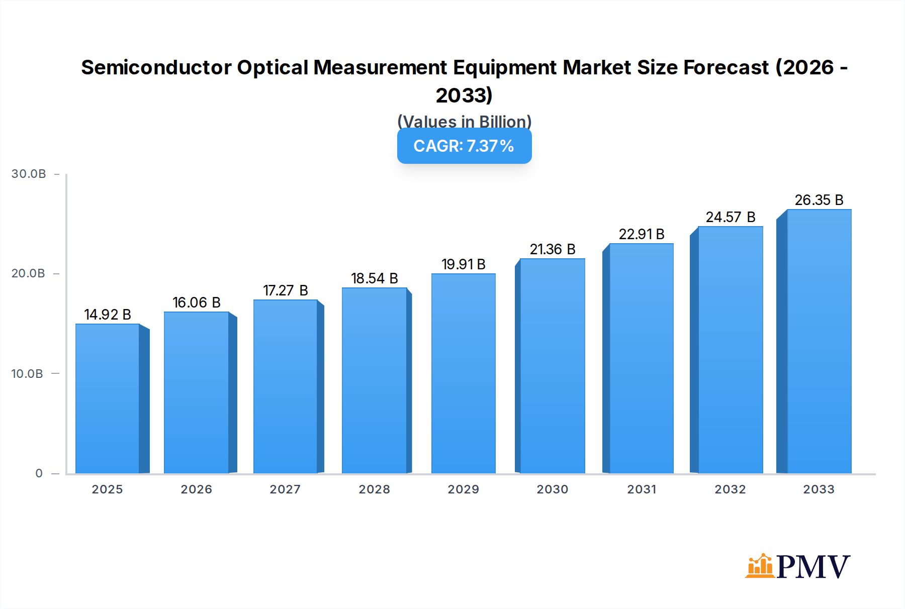
Semiconductor Optical Measurement Equipment Market Size (In Billion)

Emerging trends like the adoption of AI and machine learning for automated defect detection and analysis, alongside advancements in high-resolution optical imaging technologies, are set to revolutionize the semiconductor optical measurement landscape. These innovations promise enhanced throughput and improved defect identification capabilities, directly addressing the industry's need for greater efficiency and yield. While the market enjoys strong growth drivers, certain restraints, such as the high initial investment cost of sophisticated metrology equipment and the stringent calibration requirements, could pose challenges. However, the continuous innovation from leading players like KLA Corporation, Applied Materials, and ASML, coupled with the expanding applications in wafer inspection and mask/film inspection, are expected to offset these limitations. The diverse range of equipment, including Critical Dimension Measurement Equipment and 3D Morphology Measurement Equipment, caters to the intricate needs of modern semiconductor fabrication processes, ensuring the market's continued upward trajectory.

Semiconductor Optical Measurement Equipment Company Market Share
This comprehensive report delves into the dynamic global market for Semiconductor Optical Measurement Equipment, providing in-depth analysis and strategic insights for industry stakeholders. Covering the historical period from 2019 to 2024, the base year of 2025, and extending to a detailed forecast period of 2025–2033, this report equips you with the knowledge to navigate this critical sector.
Semiconductor Optical Measurement Equipment Market Structure & Competitive Dynamics
The semiconductor optical measurement equipment market is characterized by a moderate to high degree of concentration, with key players like KLA Corporation, Applied Materials, and ASML holding significant market share, estimated to be in the billions of dollars. These dominant entities drive innovation through substantial R&D investments, fostering vibrant innovation ecosystems. Regulatory frameworks, while evolving to ensure quality and standards, generally support technological advancement. The emergence of advanced materials and miniaturization in semiconductor manufacturing necessitates continuous innovation in measurement techniques, limiting the impact of product substitutes. End-user trends indicate a growing demand for higher precision, faster throughput, and integrated solutions, pushing equipment manufacturers to develop more sophisticated technologies. Merger and acquisition (M&A) activities are strategic, aimed at expanding product portfolios and geographical reach, with significant M&A deal values often in the billions. Recent M&A activities have seen companies like Onto Innovation and Camtek strategically enhancing their offerings in areas such as metrology and inspection. The market is projected to reach a valuation exceeding ten billion dollars by 2033.
Semiconductor Optical Measurement Equipment Industry Trends & Insights
The global Semiconductor Optical Measurement Equipment market is experiencing robust growth, driven by the insatiable demand for advanced semiconductors across various sectors, including artificial intelligence, 5G, automotive, and consumer electronics. The relentless pursuit of smaller feature sizes and increased chip complexity in semiconductor fabrication is a primary growth driver, necessitating increasingly sophisticated metrology and inspection solutions. Technological disruptions, such as the adoption of Extreme Ultraviolet (EUV) lithography, are creating new frontiers for optical measurement, demanding equipment capable of higher resolution and precision. Consumer preferences for faster, more powerful, and energy-efficient electronic devices directly translate into a need for more advanced semiconductor manufacturing processes, thereby fueling the demand for cutting-edge optical measurement equipment. Competitive dynamics are intense, with companies continuously investing in R&D to develop next-generation metrology and inspection systems. The projected Compound Annual Growth Rate (CAGR) for this market is approximately XX%, indicating a strong upward trajectory. Market penetration is expected to deepen as more foundries and fabs worldwide adopt advanced manufacturing techniques and the need for stringent quality control intensifies. The increasing complexity of semiconductor devices, with billions of transistors on a single chip, necessitates highly accurate optical measurement to ensure yield and performance. The global market size is expected to surpass forty billion dollars by the end of the forecast period, with significant contributions from advancements in wafer inspection and critical dimension measurement.
Dominant Markets & Segments in Semiconductor Optical Measurement Equipment
The Wafer Inspection segment, encompassing both defect inspection and metrology, stands as a dominant force within the Semiconductor Optical Measurement Equipment market. This dominance is fueled by the fundamental need to ensure the highest possible yield in semiconductor manufacturing. Foundries and Integrated Device Manufacturers (IDMs) across the globe are heavily invested in advanced wafer inspection techniques to identify and mitigate defects at every stage of the fabrication process.
- Key Drivers of Wafer Inspection Dominance:
- Economic Policies: Government initiatives promoting semiconductor self-sufficiency and R&D investment in key regions like the United States, Europe, and Asia are driving fab expansions and, consequently, the demand for inspection equipment.
- Infrastructure: The construction of new, state-of-the-art semiconductor fabrication plants (fabs) worldwide, requiring billions in investment, directly translates to a substantial need for wafer inspection solutions.
- Technological Advancements: The continuous drive for smaller nodes (e.g., 3nm, 2nm) in semiconductor manufacturing introduces new defect types and requires highly advanced optical metrology and inspection capabilities.
- Yield Optimization: Maximizing chip yield is paramount in semiconductor manufacturing, where even minor defects can lead to billions in lost revenue. Robust wafer inspection is crucial for achieving this.
Within the Types of optical measurement equipment, Critical Dimension (CD) Measurement Equipment exhibits significant market penetration. The ability to accurately measure critical dimensions, often at the nanometer scale, is indispensable for controlling device performance and ensuring process repeatability.
- Dominance of CD Measurement Equipment:
- Lithography Control: Accurate CD measurement is vital for controlling the outcomes of photolithography processes, a cornerstone of semiconductor manufacturing.
- Process Control: It enables real-time process adjustments, preventing deviations that could lead to yield loss.
- Advanced Node Requirements: As semiconductor nodes shrink, the precision required for CD measurement increases exponentially, making this segment indispensable for leading-edge manufacturing.
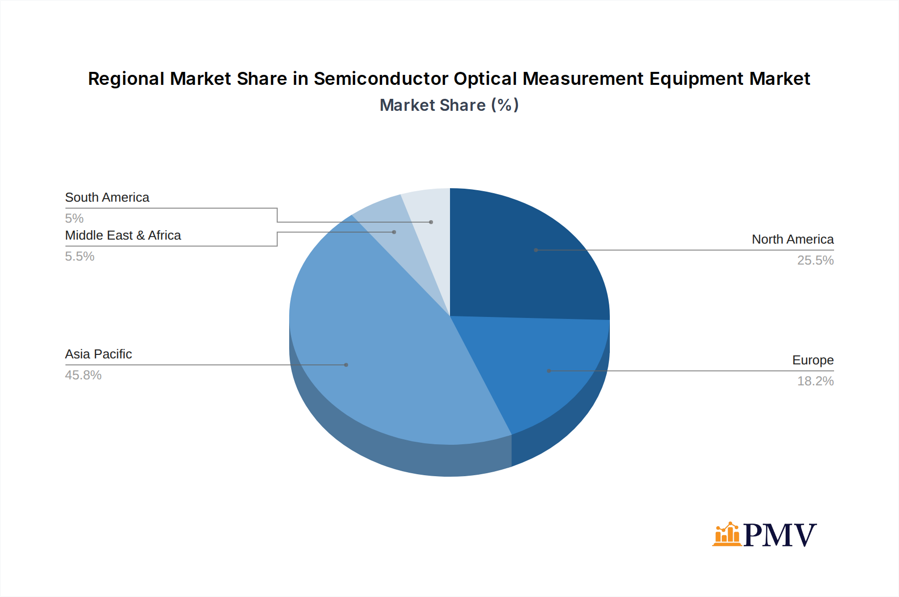
Geographically, Asia-Pacific, particularly Taiwan, South Korea, and China, represents the dominant region for Semiconductor Optical Measurement Equipment. This is due to the concentration of major semiconductor manufacturing hubs and foundries in these countries, driving substantial demand for advanced inspection and metrology solutions, estimated to account for over sixty percent of the global market.
Semiconductor Optical Measurement Equipment Product Innovations
Product innovation in Semiconductor Optical Measurement Equipment is primarily focused on enhancing resolution, speed, and automation. Companies are developing advanced optical systems that leverage machine learning and artificial intelligence to improve defect detection accuracy and reduce false positives. Key innovations include multi-wavelength imaging for enhanced material characterization and 3D metrology techniques for precise surface profiling. These advancements offer significant competitive advantages by enabling manufacturers to achieve higher yields, reduce production costs, and accelerate time-to-market for next-generation semiconductor devices. The market is projected to see sustained innovation in areas like in-line metrology for real-time process feedback, a critical need for high-volume manufacturing.
Report Segmentation & Scope
This report segments the Semiconductor Optical Measurement Equipment market across key applications and equipment types. The Application segments include Wafer Inspection and Mask/Film Inspection. The Types segments encompass Overlay Precision Measuring Equipment, Wafer Dielectric Thin Film Measurement Equipment, Critical Dimension Measurement Equipment, 3D Morphology Measurement Equipment, and Others. The Wafer Inspection segment is projected to hold a significant market share exceeding twenty billion dollars by 2033, driven by increasing fab capacity and the need for defect reduction. Mask/Film Inspection, while smaller, is crucial for ensuring the integrity of photomasks and films used in lithography. Within the Types, Critical Dimension Measurement Equipment is expected to witness strong growth due to shrinking nodes. 3D Morphology Measurement Equipment is gaining traction for advanced packaging and surface analysis.
Key Drivers of Semiconductor Optical Measurement Equipment Growth
The growth of the Semiconductor Optical Measurement Equipment market is propelled by several key factors. The escalating demand for advanced semiconductors in AI, IoT, and automotive applications is a primary catalyst. The relentless drive towards smaller, more powerful, and energy-efficient chips necessitates sophisticated metrology to ensure precision and yield. Furthermore, stringent quality control standards and the high cost of semiconductor manufacturing defects incentivize investment in advanced inspection and measurement tools. Government initiatives supporting domestic semiconductor production also contribute significantly to market expansion, fostering billions in new fab investments.
Challenges in the Semiconductor Optical Measurement Equipment Sector
Despite robust growth, the Semiconductor Optical Measurement Equipment sector faces several challenges. The extremely high cost of cutting-edge equipment, often running into hundreds of millions of dollars per system, can be a barrier for smaller manufacturers. Intense competition among established players and emerging innovators, coupled with the rapid pace of technological evolution, requires continuous and substantial R&D investment. Supply chain disruptions, particularly for specialized components and materials, can impact production timelines and costs. Furthermore, the increasing complexity of semiconductor manufacturing processes presents ongoing challenges in developing and validating new measurement techniques, demanding highly skilled personnel and significant calibration efforts.
Leading Players in the Semiconductor Optical Measurement Equipment Market
- KLA Corporation
- Applied Materials
- Hitachi High-Tech
- ASML
- NanoSystem Solutions
- Onto Innovation
- Takano Corporation
- Lasertec
- Advantest
- SCREEN Holdings
- Camtek
- Toray Engineering
- Mue Tec
- Unity Semiconductor SAS
- Nordson Corporation
- Skyverse Technology
- Wuhan Jingce Electronic Group
- RSIC
Key Developments in Semiconductor Optical Measurement Equipment Sector
- 2023: KLA Corporation launched new advanced inspection systems for advanced packaging, addressing critical dimensional challenges and defect detection for next-generation chip designs.
- 2023: Applied Materials introduced novel metrology solutions to enhance yield and process control for 3D NAND flash memory manufacturing.
- 2023: Onto Innovation expanded its portfolio with acquisitions aimed at strengthening its position in inspection and metrology for advanced semiconductor nodes, with deal values reaching billions.
- 2024: Lasertec announced advancements in EUV mask inspection technology, crucial for enabling next-generation lithography processes and ensuring mask integrity.
- 2024: ASML continued to innovate in metrology for its EUV lithography systems, aiming to improve critical dimension control and reduce process variations, impacting billions in wafer production.
Strategic Semiconductor Optical Measurement Equipment Market Outlook
The strategic outlook for the Semiconductor Optical Measurement Equipment market remains highly positive, driven by sustained demand for advanced semiconductors and continuous technological innovation. Growth accelerators include the burgeoning AI and machine learning industries, the ongoing miniaturization of semiconductor components, and the increasing adoption of heterogeneous integration and advanced packaging techniques. Strategic opportunities lie in developing integrated metrology solutions, AI-powered analytics for defect prediction, and solutions tailored for emerging applications like quantum computing and advanced sensors. Companies that can offer higher precision, faster throughput, and more comprehensive data analysis will be best positioned to capitalize on the projected market growth, expected to reach billions in investment over the next decade.
Semiconductor Optical Measurement Equipment Segmentation
-
1. Application
- 1.1. Wafer Inspection
- 1.2. Mask/Film Inspection
-
2. Types
- 2.1. Overlay Precision Measuring Equipment
- 2.2. Wafer Dielectric Thin Film Measurement Equipment
- 2.3. Critical Dimension Measurement Equipment
- 2.4. 3D Morphology Measurement Equipment
- 2.5. Others
Semiconductor Optical Measurement Equipment Segmentation By Geography
-
1. North America
- 1.1. United States
- 1.2. Canada
- 1.3. Mexico
-
2. South America
- 2.1. Brazil
- 2.2. Argentina
- 2.3. Rest of South America
-
3. Europe
- 3.1. United Kingdom
- 3.2. Germany
- 3.3. France
- 3.4. Italy
- 3.5. Spain
- 3.6. Russia
- 3.7. Benelux
- 3.8. Nordics
- 3.9. Rest of Europe
-
4. Middle East & Africa
- 4.1. Turkey
- 4.2. Israel
- 4.3. GCC
- 4.4. North Africa
- 4.5. South Africa
- 4.6. Rest of Middle East & Africa
-
5. Asia Pacific
- 5.1. China
- 5.2. India
- 5.3. Japan
- 5.4. South Korea
- 5.5. ASEAN
- 5.6. Oceania
- 5.7. Rest of Asia Pacific
Semiconductor Optical Measurement Equipment Regional Market Share
Geographic Coverage of Semiconductor Optical Measurement Equipment
Semiconductor Optical Measurement Equipment REPORT HIGHLIGHTS
| Aspects | Details |
|---|---|
| Study Period | 2020-2034 |
| Base Year | 2025 |
| Estimated Year | 2026 |
| Forecast Period | 2026-2034 |
| Historical Period | 2020-2025 |
| Growth Rate | CAGR of 6.9% from 2020-2034 |
| Segmentation |
|
Table of Contents
- 1. Introduction
- 1.1. Research Scope
- 1.2. Market Segmentation
- 1.3. Research Methodology
- 1.4. Definitions and Assumptions
- 2. Executive Summary
- 2.1. Introduction
- 3. Market Dynamics
- 3.1. Introduction
- 3.2. Market Drivers
- 3.3. Market Restrains
- 3.4. Market Trends
- 4. Market Factor Analysis
- 4.1. Porters Five Forces
- 4.2. Supply/Value Chain
- 4.3. PESTEL analysis
- 4.4. Market Entropy
- 4.5. Patent/Trademark Analysis
- 5. Global Semiconductor Optical Measurement Equipment Analysis, Insights and Forecast, 2020-2032
- 5.1. Market Analysis, Insights and Forecast - by Application
- 5.1.1. Wafer Inspection
- 5.1.2. Mask/Film Inspection
- 5.2. Market Analysis, Insights and Forecast - by Types
- 5.2.1. Overlay Precision Measuring Equipment
- 5.2.2. Wafer Dielectric Thin Film Measurement Equipment
- 5.2.3. Critical Dimension Measurement Equipment
- 5.2.4. 3D Morphology Measurement Equipment
- 5.2.5. Others
- 5.3. Market Analysis, Insights and Forecast - by Region
- 5.3.1. North America
- 5.3.2. South America
- 5.3.3. Europe
- 5.3.4. Middle East & Africa
- 5.3.5. Asia Pacific
- 5.1. Market Analysis, Insights and Forecast - by Application
- 6. North America Semiconductor Optical Measurement Equipment Analysis, Insights and Forecast, 2020-2032
- 6.1. Market Analysis, Insights and Forecast - by Application
- 6.1.1. Wafer Inspection
- 6.1.2. Mask/Film Inspection
- 6.2. Market Analysis, Insights and Forecast - by Types
- 6.2.1. Overlay Precision Measuring Equipment
- 6.2.2. Wafer Dielectric Thin Film Measurement Equipment
- 6.2.3. Critical Dimension Measurement Equipment
- 6.2.4. 3D Morphology Measurement Equipment
- 6.2.5. Others
- 6.1. Market Analysis, Insights and Forecast - by Application
- 7. South America Semiconductor Optical Measurement Equipment Analysis, Insights and Forecast, 2020-2032
- 7.1. Market Analysis, Insights and Forecast - by Application
- 7.1.1. Wafer Inspection
- 7.1.2. Mask/Film Inspection
- 7.2. Market Analysis, Insights and Forecast - by Types
- 7.2.1. Overlay Precision Measuring Equipment
- 7.2.2. Wafer Dielectric Thin Film Measurement Equipment
- 7.2.3. Critical Dimension Measurement Equipment
- 7.2.4. 3D Morphology Measurement Equipment
- 7.2.5. Others
- 7.1. Market Analysis, Insights and Forecast - by Application
- 8. Europe Semiconductor Optical Measurement Equipment Analysis, Insights and Forecast, 2020-2032
- 8.1. Market Analysis, Insights and Forecast - by Application
- 8.1.1. Wafer Inspection
- 8.1.2. Mask/Film Inspection
- 8.2. Market Analysis, Insights and Forecast - by Types
- 8.2.1. Overlay Precision Measuring Equipment
- 8.2.2. Wafer Dielectric Thin Film Measurement Equipment
- 8.2.3. Critical Dimension Measurement Equipment
- 8.2.4. 3D Morphology Measurement Equipment
- 8.2.5. Others
- 8.1. Market Analysis, Insights and Forecast - by Application
- 9. Middle East & Africa Semiconductor Optical Measurement Equipment Analysis, Insights and Forecast, 2020-2032
- 9.1. Market Analysis, Insights and Forecast - by Application
- 9.1.1. Wafer Inspection
- 9.1.2. Mask/Film Inspection
- 9.2. Market Analysis, Insights and Forecast - by Types
- 9.2.1. Overlay Precision Measuring Equipment
- 9.2.2. Wafer Dielectric Thin Film Measurement Equipment
- 9.2.3. Critical Dimension Measurement Equipment
- 9.2.4. 3D Morphology Measurement Equipment
- 9.2.5. Others
- 9.1. Market Analysis, Insights and Forecast - by Application
- 10. Asia Pacific Semiconductor Optical Measurement Equipment Analysis, Insights and Forecast, 2020-2032
- 10.1. Market Analysis, Insights and Forecast - by Application
- 10.1.1. Wafer Inspection
- 10.1.2. Mask/Film Inspection
- 10.2. Market Analysis, Insights and Forecast - by Types
- 10.2.1. Overlay Precision Measuring Equipment
- 10.2.2. Wafer Dielectric Thin Film Measurement Equipment
- 10.2.3. Critical Dimension Measurement Equipment
- 10.2.4. 3D Morphology Measurement Equipment
- 10.2.5. Others
- 10.1. Market Analysis, Insights and Forecast - by Application
- 11. Competitive Analysis
- 11.1. Global Market Share Analysis 2025
- 11.2. Company Profiles
- 11.2.1 KLA Corporation
- 11.2.1.1. Overview
- 11.2.1.2. Products
- 11.2.1.3. SWOT Analysis
- 11.2.1.4. Recent Developments
- 11.2.1.5. Financials (Based on Availability)
- 11.2.2 Applied Materials
- 11.2.2.1. Overview
- 11.2.2.2. Products
- 11.2.2.3. SWOT Analysis
- 11.2.2.4. Recent Developments
- 11.2.2.5. Financials (Based on Availability)
- 11.2.3 Hitachi High-Tech
- 11.2.3.1. Overview
- 11.2.3.2. Products
- 11.2.3.3. SWOT Analysis
- 11.2.3.4. Recent Developments
- 11.2.3.5. Financials (Based on Availability)
- 11.2.4 ASML
- 11.2.4.1. Overview
- 11.2.4.2. Products
- 11.2.4.3. SWOT Analysis
- 11.2.4.4. Recent Developments
- 11.2.4.5. Financials (Based on Availability)
- 11.2.5 NanoSystem Solutions
- 11.2.5.1. Overview
- 11.2.5.2. Products
- 11.2.5.3. SWOT Analysis
- 11.2.5.4. Recent Developments
- 11.2.5.5. Financials (Based on Availability)
- 11.2.6 Onto Innovation
- 11.2.6.1. Overview
- 11.2.6.2. Products
- 11.2.6.3. SWOT Analysis
- 11.2.6.4. Recent Developments
- 11.2.6.5. Financials (Based on Availability)
- 11.2.7 Takano Corporation
- 11.2.7.1. Overview
- 11.2.7.2. Products
- 11.2.7.3. SWOT Analysis
- 11.2.7.4. Recent Developments
- 11.2.7.5. Financials (Based on Availability)
- 11.2.8 Lasertec
- 11.2.8.1. Overview
- 11.2.8.2. Products
- 11.2.8.3. SWOT Analysis
- 11.2.8.4. Recent Developments
- 11.2.8.5. Financials (Based on Availability)
- 11.2.9 Advantest
- 11.2.9.1. Overview
- 11.2.9.2. Products
- 11.2.9.3. SWOT Analysis
- 11.2.9.4. Recent Developments
- 11.2.9.5. Financials (Based on Availability)
- 11.2.10 SCREEN Holdings
- 11.2.10.1. Overview
- 11.2.10.2. Products
- 11.2.10.3. SWOT Analysis
- 11.2.10.4. Recent Developments
- 11.2.10.5. Financials (Based on Availability)
- 11.2.11 Camtek
- 11.2.11.1. Overview
- 11.2.11.2. Products
- 11.2.11.3. SWOT Analysis
- 11.2.11.4. Recent Developments
- 11.2.11.5. Financials (Based on Availability)
- 11.2.12 Toray Engineering
- 11.2.12.1. Overview
- 11.2.12.2. Products
- 11.2.12.3. SWOT Analysis
- 11.2.12.4. Recent Developments
- 11.2.12.5. Financials (Based on Availability)
- 11.2.13 Mue Tec
- 11.2.13.1. Overview
- 11.2.13.2. Products
- 11.2.13.3. SWOT Analysis
- 11.2.13.4. Recent Developments
- 11.2.13.5. Financials (Based on Availability)
- 11.2.14 Unity Semiconductor SAS
- 11.2.14.1. Overview
- 11.2.14.2. Products
- 11.2.14.3. SWOT Analysis
- 11.2.14.4. Recent Developments
- 11.2.14.5. Financials (Based on Availability)
- 11.2.15 Nordson Corporation
- 11.2.15.1. Overview
- 11.2.15.2. Products
- 11.2.15.3. SWOT Analysis
- 11.2.15.4. Recent Developments
- 11.2.15.5. Financials (Based on Availability)
- 11.2.16 Skyverse Technology
- 11.2.16.1. Overview
- 11.2.16.2. Products
- 11.2.16.3. SWOT Analysis
- 11.2.16.4. Recent Developments
- 11.2.16.5. Financials (Based on Availability)
- 11.2.17 Wuhan Jingce Electronic Group
- 11.2.17.1. Overview
- 11.2.17.2. Products
- 11.2.17.3. SWOT Analysis
- 11.2.17.4. Recent Developments
- 11.2.17.5. Financials (Based on Availability)
- 11.2.18 RSIC
- 11.2.18.1. Overview
- 11.2.18.2. Products
- 11.2.18.3. SWOT Analysis
- 11.2.18.4. Recent Developments
- 11.2.18.5. Financials (Based on Availability)
- 11.2.1 KLA Corporation
List of Figures
- Figure 1: Global Semiconductor Optical Measurement Equipment Revenue Breakdown (billion, %) by Region 2025 & 2033
- Figure 2: Global Semiconductor Optical Measurement Equipment Volume Breakdown (K, %) by Region 2025 & 2033
- Figure 3: North America Semiconductor Optical Measurement Equipment Revenue (billion), by Application 2025 & 2033
- Figure 4: North America Semiconductor Optical Measurement Equipment Volume (K), by Application 2025 & 2033
- Figure 5: North America Semiconductor Optical Measurement Equipment Revenue Share (%), by Application 2025 & 2033
- Figure 6: North America Semiconductor Optical Measurement Equipment Volume Share (%), by Application 2025 & 2033
- Figure 7: North America Semiconductor Optical Measurement Equipment Revenue (billion), by Types 2025 & 2033
- Figure 8: North America Semiconductor Optical Measurement Equipment Volume (K), by Types 2025 & 2033
- Figure 9: North America Semiconductor Optical Measurement Equipment Revenue Share (%), by Types 2025 & 2033
- Figure 10: North America Semiconductor Optical Measurement Equipment Volume Share (%), by Types 2025 & 2033
- Figure 11: North America Semiconductor Optical Measurement Equipment Revenue (billion), by Country 2025 & 2033
- Figure 12: North America Semiconductor Optical Measurement Equipment Volume (K), by Country 2025 & 2033
- Figure 13: North America Semiconductor Optical Measurement Equipment Revenue Share (%), by Country 2025 & 2033
- Figure 14: North America Semiconductor Optical Measurement Equipment Volume Share (%), by Country 2025 & 2033
- Figure 15: South America Semiconductor Optical Measurement Equipment Revenue (billion), by Application 2025 & 2033
- Figure 16: South America Semiconductor Optical Measurement Equipment Volume (K), by Application 2025 & 2033
- Figure 17: South America Semiconductor Optical Measurement Equipment Revenue Share (%), by Application 2025 & 2033
- Figure 18: South America Semiconductor Optical Measurement Equipment Volume Share (%), by Application 2025 & 2033
- Figure 19: South America Semiconductor Optical Measurement Equipment Revenue (billion), by Types 2025 & 2033
- Figure 20: South America Semiconductor Optical Measurement Equipment Volume (K), by Types 2025 & 2033
- Figure 21: South America Semiconductor Optical Measurement Equipment Revenue Share (%), by Types 2025 & 2033
- Figure 22: South America Semiconductor Optical Measurement Equipment Volume Share (%), by Types 2025 & 2033
- Figure 23: South America Semiconductor Optical Measurement Equipment Revenue (billion), by Country 2025 & 2033
- Figure 24: South America Semiconductor Optical Measurement Equipment Volume (K), by Country 2025 & 2033
- Figure 25: South America Semiconductor Optical Measurement Equipment Revenue Share (%), by Country 2025 & 2033
- Figure 26: South America Semiconductor Optical Measurement Equipment Volume Share (%), by Country 2025 & 2033
- Figure 27: Europe Semiconductor Optical Measurement Equipment Revenue (billion), by Application 2025 & 2033
- Figure 28: Europe Semiconductor Optical Measurement Equipment Volume (K), by Application 2025 & 2033
- Figure 29: Europe Semiconductor Optical Measurement Equipment Revenue Share (%), by Application 2025 & 2033
- Figure 30: Europe Semiconductor Optical Measurement Equipment Volume Share (%), by Application 2025 & 2033
- Figure 31: Europe Semiconductor Optical Measurement Equipment Revenue (billion), by Types 2025 & 2033
- Figure 32: Europe Semiconductor Optical Measurement Equipment Volume (K), by Types 2025 & 2033
- Figure 33: Europe Semiconductor Optical Measurement Equipment Revenue Share (%), by Types 2025 & 2033
- Figure 34: Europe Semiconductor Optical Measurement Equipment Volume Share (%), by Types 2025 & 2033
- Figure 35: Europe Semiconductor Optical Measurement Equipment Revenue (billion), by Country 2025 & 2033
- Figure 36: Europe Semiconductor Optical Measurement Equipment Volume (K), by Country 2025 & 2033
- Figure 37: Europe Semiconductor Optical Measurement Equipment Revenue Share (%), by Country 2025 & 2033
- Figure 38: Europe Semiconductor Optical Measurement Equipment Volume Share (%), by Country 2025 & 2033
- Figure 39: Middle East & Africa Semiconductor Optical Measurement Equipment Revenue (billion), by Application 2025 & 2033
- Figure 40: Middle East & Africa Semiconductor Optical Measurement Equipment Volume (K), by Application 2025 & 2033
- Figure 41: Middle East & Africa Semiconductor Optical Measurement Equipment Revenue Share (%), by Application 2025 & 2033
- Figure 42: Middle East & Africa Semiconductor Optical Measurement Equipment Volume Share (%), by Application 2025 & 2033
- Figure 43: Middle East & Africa Semiconductor Optical Measurement Equipment Revenue (billion), by Types 2025 & 2033
- Figure 44: Middle East & Africa Semiconductor Optical Measurement Equipment Volume (K), by Types 2025 & 2033
- Figure 45: Middle East & Africa Semiconductor Optical Measurement Equipment Revenue Share (%), by Types 2025 & 2033
- Figure 46: Middle East & Africa Semiconductor Optical Measurement Equipment Volume Share (%), by Types 2025 & 2033
- Figure 47: Middle East & Africa Semiconductor Optical Measurement Equipment Revenue (billion), by Country 2025 & 2033
- Figure 48: Middle East & Africa Semiconductor Optical Measurement Equipment Volume (K), by Country 2025 & 2033
- Figure 49: Middle East & Africa Semiconductor Optical Measurement Equipment Revenue Share (%), by Country 2025 & 2033
- Figure 50: Middle East & Africa Semiconductor Optical Measurement Equipment Volume Share (%), by Country 2025 & 2033
- Figure 51: Asia Pacific Semiconductor Optical Measurement Equipment Revenue (billion), by Application 2025 & 2033
- Figure 52: Asia Pacific Semiconductor Optical Measurement Equipment Volume (K), by Application 2025 & 2033
- Figure 53: Asia Pacific Semiconductor Optical Measurement Equipment Revenue Share (%), by Application 2025 & 2033
- Figure 54: Asia Pacific Semiconductor Optical Measurement Equipment Volume Share (%), by Application 2025 & 2033
- Figure 55: Asia Pacific Semiconductor Optical Measurement Equipment Revenue (billion), by Types 2025 & 2033
- Figure 56: Asia Pacific Semiconductor Optical Measurement Equipment Volume (K), by Types 2025 & 2033
- Figure 57: Asia Pacific Semiconductor Optical Measurement Equipment Revenue Share (%), by Types 2025 & 2033
- Figure 58: Asia Pacific Semiconductor Optical Measurement Equipment Volume Share (%), by Types 2025 & 2033
- Figure 59: Asia Pacific Semiconductor Optical Measurement Equipment Revenue (billion), by Country 2025 & 2033
- Figure 60: Asia Pacific Semiconductor Optical Measurement Equipment Volume (K), by Country 2025 & 2033
- Figure 61: Asia Pacific Semiconductor Optical Measurement Equipment Revenue Share (%), by Country 2025 & 2033
- Figure 62: Asia Pacific Semiconductor Optical Measurement Equipment Volume Share (%), by Country 2025 & 2033
List of Tables
- Table 1: Global Semiconductor Optical Measurement Equipment Revenue billion Forecast, by Application 2020 & 2033
- Table 2: Global Semiconductor Optical Measurement Equipment Volume K Forecast, by Application 2020 & 2033
- Table 3: Global Semiconductor Optical Measurement Equipment Revenue billion Forecast, by Types 2020 & 2033
- Table 4: Global Semiconductor Optical Measurement Equipment Volume K Forecast, by Types 2020 & 2033
- Table 5: Global Semiconductor Optical Measurement Equipment Revenue billion Forecast, by Region 2020 & 2033
- Table 6: Global Semiconductor Optical Measurement Equipment Volume K Forecast, by Region 2020 & 2033
- Table 7: Global Semiconductor Optical Measurement Equipment Revenue billion Forecast, by Application 2020 & 2033
- Table 8: Global Semiconductor Optical Measurement Equipment Volume K Forecast, by Application 2020 & 2033
- Table 9: Global Semiconductor Optical Measurement Equipment Revenue billion Forecast, by Types 2020 & 2033
- Table 10: Global Semiconductor Optical Measurement Equipment Volume K Forecast, by Types 2020 & 2033
- Table 11: Global Semiconductor Optical Measurement Equipment Revenue billion Forecast, by Country 2020 & 2033
- Table 12: Global Semiconductor Optical Measurement Equipment Volume K Forecast, by Country 2020 & 2033
- Table 13: United States Semiconductor Optical Measurement Equipment Revenue (billion) Forecast, by Application 2020 & 2033
- Table 14: United States Semiconductor Optical Measurement Equipment Volume (K) Forecast, by Application 2020 & 2033
- Table 15: Canada Semiconductor Optical Measurement Equipment Revenue (billion) Forecast, by Application 2020 & 2033
- Table 16: Canada Semiconductor Optical Measurement Equipment Volume (K) Forecast, by Application 2020 & 2033
- Table 17: Mexico Semiconductor Optical Measurement Equipment Revenue (billion) Forecast, by Application 2020 & 2033
- Table 18: Mexico Semiconductor Optical Measurement Equipment Volume (K) Forecast, by Application 2020 & 2033
- Table 19: Global Semiconductor Optical Measurement Equipment Revenue billion Forecast, by Application 2020 & 2033
- Table 20: Global Semiconductor Optical Measurement Equipment Volume K Forecast, by Application 2020 & 2033
- Table 21: Global Semiconductor Optical Measurement Equipment Revenue billion Forecast, by Types 2020 & 2033
- Table 22: Global Semiconductor Optical Measurement Equipment Volume K Forecast, by Types 2020 & 2033
- Table 23: Global Semiconductor Optical Measurement Equipment Revenue billion Forecast, by Country 2020 & 2033
- Table 24: Global Semiconductor Optical Measurement Equipment Volume K Forecast, by Country 2020 & 2033
- Table 25: Brazil Semiconductor Optical Measurement Equipment Revenue (billion) Forecast, by Application 2020 & 2033
- Table 26: Brazil Semiconductor Optical Measurement Equipment Volume (K) Forecast, by Application 2020 & 2033
- Table 27: Argentina Semiconductor Optical Measurement Equipment Revenue (billion) Forecast, by Application 2020 & 2033
- Table 28: Argentina Semiconductor Optical Measurement Equipment Volume (K) Forecast, by Application 2020 & 2033
- Table 29: Rest of South America Semiconductor Optical Measurement Equipment Revenue (billion) Forecast, by Application 2020 & 2033
- Table 30: Rest of South America Semiconductor Optical Measurement Equipment Volume (K) Forecast, by Application 2020 & 2033
- Table 31: Global Semiconductor Optical Measurement Equipment Revenue billion Forecast, by Application 2020 & 2033
- Table 32: Global Semiconductor Optical Measurement Equipment Volume K Forecast, by Application 2020 & 2033
- Table 33: Global Semiconductor Optical Measurement Equipment Revenue billion Forecast, by Types 2020 & 2033
- Table 34: Global Semiconductor Optical Measurement Equipment Volume K Forecast, by Types 2020 & 2033
- Table 35: Global Semiconductor Optical Measurement Equipment Revenue billion Forecast, by Country 2020 & 2033
- Table 36: Global Semiconductor Optical Measurement Equipment Volume K Forecast, by Country 2020 & 2033
- Table 37: United Kingdom Semiconductor Optical Measurement Equipment Revenue (billion) Forecast, by Application 2020 & 2033
- Table 38: United Kingdom Semiconductor Optical Measurement Equipment Volume (K) Forecast, by Application 2020 & 2033
- Table 39: Germany Semiconductor Optical Measurement Equipment Revenue (billion) Forecast, by Application 2020 & 2033
- Table 40: Germany Semiconductor Optical Measurement Equipment Volume (K) Forecast, by Application 2020 & 2033
- Table 41: France Semiconductor Optical Measurement Equipment Revenue (billion) Forecast, by Application 2020 & 2033
- Table 42: France Semiconductor Optical Measurement Equipment Volume (K) Forecast, by Application 2020 & 2033
- Table 43: Italy Semiconductor Optical Measurement Equipment Revenue (billion) Forecast, by Application 2020 & 2033
- Table 44: Italy Semiconductor Optical Measurement Equipment Volume (K) Forecast, by Application 2020 & 2033
- Table 45: Spain Semiconductor Optical Measurement Equipment Revenue (billion) Forecast, by Application 2020 & 2033
- Table 46: Spain Semiconductor Optical Measurement Equipment Volume (K) Forecast, by Application 2020 & 2033
- Table 47: Russia Semiconductor Optical Measurement Equipment Revenue (billion) Forecast, by Application 2020 & 2033
- Table 48: Russia Semiconductor Optical Measurement Equipment Volume (K) Forecast, by Application 2020 & 2033
- Table 49: Benelux Semiconductor Optical Measurement Equipment Revenue (billion) Forecast, by Application 2020 & 2033
- Table 50: Benelux Semiconductor Optical Measurement Equipment Volume (K) Forecast, by Application 2020 & 2033
- Table 51: Nordics Semiconductor Optical Measurement Equipment Revenue (billion) Forecast, by Application 2020 & 2033
- Table 52: Nordics Semiconductor Optical Measurement Equipment Volume (K) Forecast, by Application 2020 & 2033
- Table 53: Rest of Europe Semiconductor Optical Measurement Equipment Revenue (billion) Forecast, by Application 2020 & 2033
- Table 54: Rest of Europe Semiconductor Optical Measurement Equipment Volume (K) Forecast, by Application 2020 & 2033
- Table 55: Global Semiconductor Optical Measurement Equipment Revenue billion Forecast, by Application 2020 & 2033
- Table 56: Global Semiconductor Optical Measurement Equipment Volume K Forecast, by Application 2020 & 2033
- Table 57: Global Semiconductor Optical Measurement Equipment Revenue billion Forecast, by Types 2020 & 2033
- Table 58: Global Semiconductor Optical Measurement Equipment Volume K Forecast, by Types 2020 & 2033
- Table 59: Global Semiconductor Optical Measurement Equipment Revenue billion Forecast, by Country 2020 & 2033
- Table 60: Global Semiconductor Optical Measurement Equipment Volume K Forecast, by Country 2020 & 2033
- Table 61: Turkey Semiconductor Optical Measurement Equipment Revenue (billion) Forecast, by Application 2020 & 2033
- Table 62: Turkey Semiconductor Optical Measurement Equipment Volume (K) Forecast, by Application 2020 & 2033
- Table 63: Israel Semiconductor Optical Measurement Equipment Revenue (billion) Forecast, by Application 2020 & 2033
- Table 64: Israel Semiconductor Optical Measurement Equipment Volume (K) Forecast, by Application 2020 & 2033
- Table 65: GCC Semiconductor Optical Measurement Equipment Revenue (billion) Forecast, by Application 2020 & 2033
- Table 66: GCC Semiconductor Optical Measurement Equipment Volume (K) Forecast, by Application 2020 & 2033
- Table 67: North Africa Semiconductor Optical Measurement Equipment Revenue (billion) Forecast, by Application 2020 & 2033
- Table 68: North Africa Semiconductor Optical Measurement Equipment Volume (K) Forecast, by Application 2020 & 2033
- Table 69: South Africa Semiconductor Optical Measurement Equipment Revenue (billion) Forecast, by Application 2020 & 2033
- Table 70: South Africa Semiconductor Optical Measurement Equipment Volume (K) Forecast, by Application 2020 & 2033
- Table 71: Rest of Middle East & Africa Semiconductor Optical Measurement Equipment Revenue (billion) Forecast, by Application 2020 & 2033
- Table 72: Rest of Middle East & Africa Semiconductor Optical Measurement Equipment Volume (K) Forecast, by Application 2020 & 2033
- Table 73: Global Semiconductor Optical Measurement Equipment Revenue billion Forecast, by Application 2020 & 2033
- Table 74: Global Semiconductor Optical Measurement Equipment Volume K Forecast, by Application 2020 & 2033
- Table 75: Global Semiconductor Optical Measurement Equipment Revenue billion Forecast, by Types 2020 & 2033
- Table 76: Global Semiconductor Optical Measurement Equipment Volume K Forecast, by Types 2020 & 2033
- Table 77: Global Semiconductor Optical Measurement Equipment Revenue billion Forecast, by Country 2020 & 2033
- Table 78: Global Semiconductor Optical Measurement Equipment Volume K Forecast, by Country 2020 & 2033
- Table 79: China Semiconductor Optical Measurement Equipment Revenue (billion) Forecast, by Application 2020 & 2033
- Table 80: China Semiconductor Optical Measurement Equipment Volume (K) Forecast, by Application 2020 & 2033
- Table 81: India Semiconductor Optical Measurement Equipment Revenue (billion) Forecast, by Application 2020 & 2033
- Table 82: India Semiconductor Optical Measurement Equipment Volume (K) Forecast, by Application 2020 & 2033
- Table 83: Japan Semiconductor Optical Measurement Equipment Revenue (billion) Forecast, by Application 2020 & 2033
- Table 84: Japan Semiconductor Optical Measurement Equipment Volume (K) Forecast, by Application 2020 & 2033
- Table 85: South Korea Semiconductor Optical Measurement Equipment Revenue (billion) Forecast, by Application 2020 & 2033
- Table 86: South Korea Semiconductor Optical Measurement Equipment Volume (K) Forecast, by Application 2020 & 2033
- Table 87: ASEAN Semiconductor Optical Measurement Equipment Revenue (billion) Forecast, by Application 2020 & 2033
- Table 88: ASEAN Semiconductor Optical Measurement Equipment Volume (K) Forecast, by Application 2020 & 2033
- Table 89: Oceania Semiconductor Optical Measurement Equipment Revenue (billion) Forecast, by Application 2020 & 2033
- Table 90: Oceania Semiconductor Optical Measurement Equipment Volume (K) Forecast, by Application 2020 & 2033
- Table 91: Rest of Asia Pacific Semiconductor Optical Measurement Equipment Revenue (billion) Forecast, by Application 2020 & 2033
- Table 92: Rest of Asia Pacific Semiconductor Optical Measurement Equipment Volume (K) Forecast, by Application 2020 & 2033
Frequently Asked Questions
1. What is the projected Compound Annual Growth Rate (CAGR) of the Semiconductor Optical Measurement Equipment?
The projected CAGR is approximately 6.9%.
2. Which companies are prominent players in the Semiconductor Optical Measurement Equipment?
Key companies in the market include KLA Corporation, Applied Materials, Hitachi High-Tech, ASML, NanoSystem Solutions, Onto Innovation, Takano Corporation, Lasertec, Advantest, SCREEN Holdings, Camtek, Toray Engineering, Mue Tec, Unity Semiconductor SAS, Nordson Corporation, Skyverse Technology, Wuhan Jingce Electronic Group, RSIC.
3. What are the main segments of the Semiconductor Optical Measurement Equipment?
The market segments include Application, Types.
4. Can you provide details about the market size?
The market size is estimated to be USD 14.92 billion as of 2022.
5. What are some drivers contributing to market growth?
N/A
6. What are the notable trends driving market growth?
N/A
7. Are there any restraints impacting market growth?
N/A
8. Can you provide examples of recent developments in the market?
N/A
9. What pricing options are available for accessing the report?
Pricing options include single-user, multi-user, and enterprise licenses priced at USD 3950.00, USD 5925.00, and USD 7900.00 respectively.
10. Is the market size provided in terms of value or volume?
The market size is provided in terms of value, measured in billion and volume, measured in K.
11. Are there any specific market keywords associated with the report?
Yes, the market keyword associated with the report is "Semiconductor Optical Measurement Equipment," which aids in identifying and referencing the specific market segment covered.
12. How do I determine which pricing option suits my needs best?
The pricing options vary based on user requirements and access needs. Individual users may opt for single-user licenses, while businesses requiring broader access may choose multi-user or enterprise licenses for cost-effective access to the report.
13. Are there any additional resources or data provided in the Semiconductor Optical Measurement Equipment report?
While the report offers comprehensive insights, it's advisable to review the specific contents or supplementary materials provided to ascertain if additional resources or data are available.
14. How can I stay updated on further developments or reports in the Semiconductor Optical Measurement Equipment?
To stay informed about further developments, trends, and reports in the Semiconductor Optical Measurement Equipment, consider subscribing to industry newsletters, following relevant companies and organizations, or regularly checking reputable industry news sources and publications.
Methodology
Step 1 - Identification of Relevant Samples Size from Population Database


Step 2 - Approaches for Defining Global Market Size (Value, Volume* & Price*)

Note*: In applicable scenarios
Step 3 - Data Sources
Primary Research
- Web Analytics
- Survey Reports
- Research Institute
- Latest Research Reports
- Opinion Leaders
Secondary Research
- Annual Reports
- White Paper
- Latest Press Release
- Industry Association
- Paid Database
- Investor Presentations

Step 4 - Data Triangulation
Involves using different sources of information in order to increase the validity of a study
These sources are likely to be stakeholders in a program - participants, other researchers, program staff, other community members, and so on.
Then we put all data in single framework & apply various statistical tools to find out the dynamic on the market.
During the analysis stage, feedback from the stakeholder groups would be compared to determine areas of agreement as well as areas of divergence