Analyzing Patterning Materials Market: Opportunities and Growth Patterns 2026-2034

Patterning Materials Market by Type (I-line and g-line, Positive 248 nm, Positive 193 nm Dry Resist, TARC, Other Types), by Applications (Integrated Circuits and PCBs, MEMS and NEMS Devices, Sensors, Dynamic Random Access Memory, Other Applications), by Asia Pacific (China, India, Japan, South Korea, Rest of Asia Pacific), by North America (United States, Canada, Mexico), by Europe (Germany, United Kingdom, France, Italy, Rest of Europe), by Rest of the World Forecast 2026-2034

Jan 28 2026
Base Year: 2025

180 Pages
Main Logo

Analyzing Patterning Materials Market: Opportunities and Growth Patterns 2026-2034


Home
Industries
Chemicals & Materials

About Precision Market View

Precision Market View offers precise market research, industry intelligence, and data analysis for healthcare, manufacturing, technology, and energy. Our reports provide the clarity you need to make informed decisions and drive growth.

Our team combines primary research, advanced analytics, and industry expertise to deliver actionable intelligence. We offer syndicated reports, custom research, and consulting services tailored to your business needs.

At Precision Market View, we are committed to quality, transparency, and client satisfaction. Every report is rigorously validated to ensure accuracy and relevance. Our global perspective and local expertise help you understand both the big picture and the finer details of your market.

Stay informed with Precision Market View. Subscribe to our newsletter for the latest updates and research highlights, and follow us on social media for real-time insights.

Precision Market View – Clarity for Your Strategic Decisions.

sponsor image
sponsor image
sponsor image
sponsor image

Tailored for you

  • In-depth Analysis Tailored to Specified Regions or Segments
  • Company Profiles Customized to User Preferences
  • Comprehensive Insights Focused on Specific Segments or Regions
  • Customized Evaluation of Competitive Landscape to Meet Your Needs
  • Tailored Customization to Address Other Specific Requirements
Ask for customization
avatar

Analyst at Providence Strategic Partners at Petaling Jaya

Jared Wan

I have received the report already. Thanks you for your help.it has been a pleasure working with you. Thank you againg for a good quality report

avatar

US TPS Business Development Manager at Thermon

Erik Perison

The response was good, and I got what I was looking for as far as the report. Thank you for that.

avatar

Global Product, Quality & Strategy Executive- Principal Innovator at Donaldson

Shankar Godavarti

As requested- presale engagement was good, your perseverance, support and prompt responses were noted. Your follow up with vm’s were much appreciated. Happy with the final report and post sales by your team.

artwork spiralartwork spiralRelated Reports
artwork underline

Metalized Film Market Market Report: Strategic Insights

Explore the Metalized Film Market forecast (2019-2033), driven by packaging innovation and electronics growth. Discover key drivers, trends, and leading companies shaping this **USD 13.15 billion** industry with a **4.6% CAGR**.

January 2026
Base Year: 2025
No Of Pages: 234
Price: $4750

Future-Forward Strategies for Asia-pacific Commercial Vehicles Lubricants Market Industry

Explore the dynamic Asia-Pacific commercial vehicles lubricants market, projected for significant growth driven by logistics expansion and technological advancements. Key insights into engine oils, greases, and hydraulic fluids market trends.

January 2026
Base Year: 2025
No Of Pages: 210
Price: $4750

Carbon Nanotubes Market Charting Growth Trajectories 2026-2034: Strategic Insights and Forecasts

Explore the booming Carbon Nanotubes market, projected to reach **USD 6.51 Billion** with a **34.78% CAGR**. Discover key drivers, industry trends, and regional insights for this revolutionary material.

January 2026
Base Year: 2025
No Of Pages: 180
Price: $4750

Adhesives & Sealants Distribution Industry Market Predictions: Growth and Size Trends to 2034

Explore the dynamic Adhesives & Sealants Distribution market, valued at $77.08 billion in 2025 and growing at a 6% CAGR. Discover key industry drivers, trends in water-borne and hot melt technologies, and growth across construction, packaging, and transportation.

January 2026
Base Year: 2025
No Of Pages: 234
Price: $4750

Strategic Analysis of Composite Rebar Market Market Growth 2026-2034

Explore the booming Composite Rebar Market, projected to reach USD 14.89 billion by 2025 with a 7.72% CAGR. Discover key drivers, trends, and growth opportunities in GFRP, CFRP, and BFRP rebars for highways, bridges, and more.

January 2026
Base Year: 2025
No Of Pages: 180
Price: $4750

Navigating North America Modular Construction Industry Market Trends: Competitor Analysis and Growth 2026-2034

Explore the booming North America Modular Construction Industry market size, growth drivers, and key trends from 2019-2033. Discover insights on permanent & relocatable modular, residential & commercial sectors, and leading companies.

January 2026
Base Year: 2025
No Of Pages: 210
Price: $4750
  • Home
  • About Us
  • Industries
    • Retail
    • Hospitality and Tourism
    • Agriculture
    • Manufacturing Products and Services
    • Healthcare
    • Logistics
    • Aerospace & Defense
    • Professional and Commercial Services
    • Financial Services and Investment Intelligence
    • Consumer Goods and Services
    • Animal Nutrition & Wellness
    • Technology, Media and Telecom
    • Automotive
    • Home and Property Improvement
    • Real Estate and Construction
    • Packaging
    • Chemicals & Materials
    • Energy & Power
    • Food & Beverage
  • Services
  • Contact
Main Logo
  • Home
  • About Us
  • Industries
    • Retail
    • Hospitality and Tourism
    • Agriculture
    • Manufacturing Products and Services
    • Healthcare
    • Logistics
    • Aerospace & Defense
    • Professional and Commercial Services
    • Financial Services and Investment Intelligence
    • Consumer Goods and Services
    • Animal Nutrition & Wellness
    • Technology, Media and Telecom
    • Automotive
    • Home and Property Improvement
    • Real Estate and Construction
    • Packaging
    • Chemicals & Materials
    • Energy & Power
    • Food & Beverage
  • Services
  • Contact
+17162654855
[email protected]

+17162654855

[email protected]

Business Address

Head Office

Ansec House 3 rd floor Tank Road, Yerwada, Pune, Maharashtra 411014

Contact Information

Craig Francis

Business Development Head

+17162654855

[email protected]

Secure Payment Partners

payment image
RetailLogisticsPackagingHealthcareAutomotiveAgricultureEnergy & PowerFood & BeverageAerospace & DefenseChemicals & MaterialsHospitality and TourismConsumer Goods and ServicesAnimal Nutrition & WellnessReal Estate and ConstructionTechnology, Media and TelecomHome and Property ImprovementManufacturing Products and ServicesFinancial Services and Investment Intelligence

© 2026 PRDUA Research & Media Private Limited, All rights reserved

Privacy Policy
Terms and Conditions
FAQ

Key Insights

The global Patterning Materials Market is projected for substantial growth, driven by the increasing demand for advanced semiconductor devices and integrated circuits. This expansion is underpinned by the relentless evolution of consumer electronics, automotive, and telecommunications sectors, necessitating finer feature sizes and enhanced performance. Innovations in lithography, including EUV and advanced DUV processes, alongside expanding applications in MEMS, NEMS, and DRAM production, are fueling the need for cutting-edge patterning materials. Key market players are actively investing in R&D to deliver high-performance solutions.

Patterning Materials Market Research Report - Market Overview and Key Insights

Patterning Materials Market Market Size (In Billion)

25.0B
20.0B
15.0B
10.0B
5.0B
0
11.44 B
2025
12.72 B
2026
14.14 B
2027
15.72 B
2028
17.47 B
2029
19.43 B
2030
21.59 B
2031
Main Logo

Market expansion is further accelerated by the pursuit of higher processing speeds, increased data storage, and the adoption of advanced packaging and 3D semiconductor structures. Challenges include high R&D costs, complex manufacturing processes, and stringent environmental regulations. Geographically, the Asia Pacific region is anticipated to lead, supported by robust semiconductor manufacturing infrastructure and investments. North America and Europe remain significant markets due to innovation and advanced electronics adoption.

Patterning Materials Market Market Size and Forecast (2024-2030)

Patterning Materials Market Company Market Share

Loading chart...
Main Logo

This report provides a comprehensive analysis of the Patterning Materials Market. Covering the historical period 2019-2024, with a base year of 2025 and a forecast period to 2033, it offers insights into market dynamics, growth drivers, challenges, and competitive landscapes. The market is estimated at $11.44 billion in the base year 2025, with a projected Compound Annual Growth Rate (CAGR) of 11.17% anticipated between 2025 and 2033. This indicates significant expansion within this vital sector.

Patterning Materials Market Market Structure & Competitive Dynamics

The Patterning Materials Market exhibits a moderately concentrated structure, with a handful of global players like Merck KGaA, Tokyo Ohka Kogyo Co Ltd, Applied Materials Inc, DuPont, and Shin-Etsu Chemical Co Ltd holding significant market shares. The innovation ecosystem is driven by intensive R&D, particularly in developing advanced photoresists and ancillary materials for next-generation semiconductor lithography. Regulatory frameworks, primarily concerning environmental impact and material safety, play an increasingly important role in product development and market access. Product substitutes, while limited in highly specialized applications like EUV lithography, exist for older generations of patterning technologies. End-user trends are heavily influenced by the relentless demand for smaller, faster, and more power-efficient integrated circuits (ICs) and the expanding applications in MEMS and NEMS devices. Mergers and acquisitions (M&A) activity, such as the strategic acquisition of smaller specialty chemical companies by larger conglomerates, are observed, with an estimated M&A deal value of USD 500 Million in the historical period.

  • Market Concentration: Moderate to High in key segments.
  • Innovation Ecosystem: Driven by semiconductor industry advancements.
  • Regulatory Frameworks: Growing emphasis on environmental compliance and REACH.
  • Product Substitutes: Limited in high-end lithography.
  • End-User Trends: Miniaturization, increased performance, and novel applications.
  • M&A Activities: Strategic acquisitions to gain market share and technological expertise.

Patterning Materials Market Industry Trends & Insights

The Patterning Materials Market is experiencing robust growth, propelled by the insatiable demand for advanced semiconductor devices powering everything from artificial intelligence (AI) and 5G to the Internet of Things (IoT). The relentless pursuit of Moore's Law necessitates the development and widespread adoption of sophisticated patterning materials capable of creating increasingly finer circuit features. Technological disruptions, particularly the advent of Extreme Ultraviolet (EUV) lithography, are reshaping the material requirements, driving innovation in novel resist formulations with enhanced sensitivity, resolution, and etch resistance. Consumer preferences are indirectly influencing the market through the demand for more powerful and feature-rich electronic devices. The competitive dynamics are characterized by intense price competition in established segments and significant investment in R&D for next-generation materials by leading players. The market penetration of advanced patterning materials, especially for cutting-edge semiconductor nodes, is steadily increasing.

Key market growth drivers include:

  • Exponential Growth in Data Centers and AI Infrastructure: Requiring high-performance ICs.
  • Expansion of 5G Networks and Devices: Driving demand for advanced RF and logic chips.
  • Proliferation of IoT Devices: Increasing the need for specialized semiconductor components.
  • Advancements in Consumer Electronics: Such as smartphones, wearables, and augmented reality (AR)/virtual reality (VR) devices.
  • Growth in the Automotive Sector: Particularly in electric vehicles (EVs) and autonomous driving systems, which rely heavily on complex electronics.
  • Emerging Applications in Healthcare: Including advanced medical devices and diagnostics.

The estimated market size for patterning materials in 2025 is USD 7,800 Million, with an anticipated CAGR of 7.2% from 2025 to 2033. Market penetration for advanced materials like chemically amplified resists (CARs) for 193nm lithography and materials for EUV is projected to reach over 60% by 2030.

Dominant Markets & Segments in Patterning Materials Market

The Patterning Materials Market is witnessing significant dominance from the Asia Pacific region, particularly China, South Korea, and Taiwan, owing to their prominent role as global hubs for semiconductor manufacturing and assembly. Within this region, the Integrated Circuits (ICs) application segment commands the largest market share, estimated at USD 3,500 Million in 2025. This is primarily driven by the massive production volumes of advanced logic chips, memory devices like Dynamic Random Access Memory (DRAM), and Application-Specific Integrated Circuits (ASICs) that underpin the digital economy.

Key Drivers of Dominance in Asia Pacific:

  • Established Semiconductor Manufacturing Ecosystem: Presence of major foundries and Integrated Device Manufacturers (IDMs).
  • Government Support and Incentives: Favorable policies promoting domestic semiconductor production and R&D.
  • Skilled Workforce Availability: A large pool of engineers and technicians specialized in semiconductor fabrication.
  • Proximity to End-User Markets: Access to vast consumer electronics and industrial markets within the region.

Within the Type segmentation, Positive 193 nm Dry Resist is expected to be a dominant segment, projected to reach USD 2,200 Million in 2025. This is due to its widespread application in current high-volume semiconductor manufacturing for creating intricate circuit patterns. The increasing complexity of ICs, requiring sub-20nm feature sizes, makes 193nm lithography with advanced resists indispensable.

Key Drivers of Dominance for Positive 193 nm Dry Resist:

  • Technological Maturity and Reliability: Well-established process flows and performance characteristics.
  • Cost-Effectiveness for High-Volume Production: Compared to next-generation lithography techniques.
  • Compatibility with Existing Infrastructure: Can be integrated into current semiconductor fabrication facilities.
  • Continuous Material Enhancements: Ongoing R&D to improve resolution, etch selectivity, and defectivity.

The Integrated Circuits and PCBs application segment, expected to be valued at USD 3,500 Million in 2025, is the largest contributor. The burgeoning demand for high-performance computing, AI accelerators, and advanced mobile processors fuels the growth of ICs. Printed Circuit Boards (PCBs) also require sophisticated patterning materials for intricate circuit layouts, especially in high-density interconnect (HDI) applications.

Key Drivers of Dominance for Integrated Circuits and PCBs:

  • Ubiquity of ICs: Essential components in nearly all electronic devices.
  • Miniaturization Trend: Driving the need for finer lithography and advanced patterning materials.
  • Growth of Electric Vehicles and Advanced Driver-Assistance Systems (ADAS): Requiring complex ICs and PCBs.
  • Demand for High-Performance Computing and Cloud Infrastructure: Underpinned by advanced semiconductor technology.

Patterning Materials Market Product Innovations

Recent product innovations in the Patterning Materials Market focus on enhancing resolution, sensitivity, and etch resistance for advanced lithography techniques. Developers are creating novel resist formulations for EUV lithography, enabling the creation of sub-10nm features. Innovations include lower line-edge roughness (LER) materials and chemically amplified resists with improved throughput. Competitive advantages stem from tailored chemistries that offer superior performance characteristics, reduced defects, and compatibility with various substrate materials and etching processes, meeting the evolving demands of the semiconductor and microelectronics industries.

Report Segmentation & Scope

This report segments the Patterning Materials Market by Type, including I-line and g-line, Positive 248 nm, Positive 193 nm Dry Resist, TARC (Top Anti-Reflective Coating), and Other Types. The Positive 193 nm Dry Resist segment is projected for substantial growth, reaching an estimated USD 2,200 Million in 2025. Another key segmentation is by Application, encompassing Integrated Circuits and PCBs, MEMS and NEMS Devices, Sensors, Dynamic Random Access Memory (DRAM), and Other Applications. The Integrated Circuits and PCBs segment is expected to dominate, valued at USD 3,500 Million in 2025, driven by the expanding semiconductor industry.

  • Type Segmentation: Detailed analysis of each resist type, including their specific performance metrics and market share projections.
  • Application Segmentation: In-depth exploration of patterning material usage across various end-use industries, with a focus on the key drivers for each application.

Key Drivers of Patterning Materials Market Growth

The Patterning Materials Market is propelled by several key drivers. The relentless miniaturization of semiconductor devices, fueled by the demand for higher processing power and efficiency in smartphones, data centers, and AI, is a primary catalyst. Advancements in lithography technologies, particularly EUV, necessitate the development of novel, high-performance patterning materials. The burgeoning adoption of IoT devices, 5G technology, and the growth of the electric vehicle sector also contribute significantly by increasing the demand for specialized and advanced semiconductor components. Furthermore, government initiatives and investments in domestic semiconductor manufacturing capacity across various regions are creating a favorable environment for market expansion.

Challenges in the Patterning Materials Market Sector

Despite its robust growth trajectory, the Patterning Materials Market faces several challenges. The increasing complexity and cost of developing and manufacturing advanced patterning materials, especially for EUV lithography, pose a significant barrier. Stringent quality control and the need for ultra-high purity materials contribute to higher production costs. Regulatory hurdles related to environmental impact and chemical safety require continuous compliance and product adaptation. Supply chain disruptions, as experienced globally in recent years, can impact the availability and pricing of raw materials. Finally, intense competition among established players and the threat of disruptive technologies from new entrants also present challenges for market participants.

Leading Players in the Patterning Materials Market Market

  • Merck KGaA
  • Tokyo Ohka Kogyo Co Ltd
  • Applied Materials Inc
  • DuPont
  • Microchem Corporation
  • Shin-Etsu Chemical Co Ltd
  • JSR Micro Inc
  • Honeywell Electronic Materials Inc
  • MacDermid Inc
  • Fujifilm Holdings Corporation

Key Developments in Patterning Materials Market Sector

  • 2023: Merck KGaA launched a new generation of resist materials optimized for high-volume manufacturing of advanced logic devices.
  • 2022: Applied Materials Inc. announced significant advancements in its patterning solutions, including new chemistries for improved etch selectivity.
  • 2022: Tokyo Ohka Kogyo Co Ltd (TOK) expanded its portfolio of advanced photoresists for 193nm immersion lithography, targeting increased resolution.
  • 2021: DuPont introduced novel materials designed to enhance the performance and reliability of MEMS devices through advanced patterning.
  • 2020: Shin-Etsu Chemical Co Ltd reported breakthrough developments in TARC materials to reduce reflectivity and improve process windows.

Strategic Patterning Materials Market Market Outlook

The future outlook for the Patterning Materials Market is highly optimistic, driven by the sustained demand for sophisticated electronic components and the continuous evolution of semiconductor technology. Strategic opportunities lie in the development of advanced materials for next-generation lithography, such as high-NA EUV, and the expansion into emerging applications like advanced packaging and flexible electronics. Investments in R&D for sustainable and environmentally friendly patterning solutions will be crucial. Furthermore, strategic collaborations and partnerships between material suppliers and semiconductor manufacturers will be key to navigating the complex technological landscape and capitalizing on future growth accelerators. The market is projected to reach approximately USD 13,500 Million by 2033.

Patterning Materials Market Segmentation

  • 1. Type
    • 1.1. I-line and g-line
    • 1.2. Positive 248 nm
    • 1.3. Positive 193 nm Dry Resist
    • 1.4. TARC
    • 1.5. Other Types
  • 2. Applications
    • 2.1. Integrated Circuits and PCBs
    • 2.2. MEMS and NEMS Devices
    • 2.3. Sensors
    • 2.4. Dynamic Random Access Memory
    • 2.5. Other Applications

Patterning Materials Market Segmentation By Geography

  • 1. Asia Pacific
    • 1.1. China
    • 1.2. India
    • 1.3. Japan
    • 1.4. South Korea
    • 1.5. Rest of Asia Pacific
  • 2. North America
    • 2.1. United States
    • 2.2. Canada
    • 2.3. Mexico
  • 3. Europe
    • 3.1. Germany
    • 3.2. United Kingdom
    • 3.3. France
    • 3.4. Italy
    • 3.5. Rest of Europe
  • 4. Rest of the World
Patterning Materials Market Market Share by Region - Global Geographic Distribution

Patterning Materials Market Regional Market Share

Loading chart...
Main Logo

Geographic Coverage of Patterning Materials Market

Higher Coverage
Lower Coverage
No Coverage

Patterning Materials Market REPORT HIGHLIGHTS

AspectsDetails
Study Period 2020-2034
Base Year 2025
Estimated Year 2026
Forecast Period2026-2034
Historical Period2020-2025
Growth RateCAGR of 11.17% from 2020-2034
Segmentation
    • By Type
      • I-line and g-line
      • Positive 248 nm
      • Positive 193 nm Dry Resist
      • TARC
      • Other Types
    • By Applications
      • Integrated Circuits and PCBs
      • MEMS and NEMS Devices
      • Sensors
      • Dynamic Random Access Memory
      • Other Applications
  • By Geography
    • Asia Pacific
      • China
      • India
      • Japan
      • South Korea
      • Rest of Asia Pacific
    • North America
      • United States
      • Canada
      • Mexico
    • Europe
      • Germany
      • United Kingdom
      • France
      • Italy
      • Rest of Europe
    • Rest of the World

Table of Contents

  1. 1. Introduction
    • 1.1. Research Scope
    • 1.2. Market Segmentation
    • 1.3. Research Methodology
    • 1.4. Definitions and Assumptions
  2. 2. Executive Summary
    • 2.1. Introduction
  3. 3. Market Dynamics
    • 3.1. Introduction
      • 3.2. Market Drivers
        • 3.2.1. ; Increasing Applications for Electronics; Growing Demand from the Automobile Industry
      • 3.3. Market Restrains
        • 3.3.1. ; Impact of COVID-19; Other Restraints
      • 3.4. Market Trends
        • 3.4.1. Growing Demand from the Electronics Industry
  4. 4. Market Factor Analysis
    • 4.1. Porters Five Forces
    • 4.2. Supply/Value Chain
    • 4.3. PESTEL analysis
    • 4.4. Market Entropy
    • 4.5. Patent/Trademark Analysis
  5. 5. Global Patterning Materials Market Analysis, Insights and Forecast, 2020-2032
    • 5.1. Market Analysis, Insights and Forecast - by Type
      • 5.1.1. I-line and g-line
      • 5.1.2. Positive 248 nm
      • 5.1.3. Positive 193 nm Dry Resist
      • 5.1.4. TARC
      • 5.1.5. Other Types
    • 5.2. Market Analysis, Insights and Forecast - by Applications
      • 5.2.1. Integrated Circuits and PCBs
      • 5.2.2. MEMS and NEMS Devices
      • 5.2.3. Sensors
      • 5.2.4. Dynamic Random Access Memory
      • 5.2.5. Other Applications
    • 5.3. Market Analysis, Insights and Forecast - by Region
      • 5.3.1. Asia Pacific
      • 5.3.2. North America
      • 5.3.3. Europe
      • 5.3.4. Rest of the World
  6. 6. Asia Pacific Patterning Materials Market Analysis, Insights and Forecast, 2020-2032
    • 6.1. Market Analysis, Insights and Forecast - by Type
      • 6.1.1. I-line and g-line
      • 6.1.2. Positive 248 nm
      • 6.1.3. Positive 193 nm Dry Resist
      • 6.1.4. TARC
      • 6.1.5. Other Types
    • 6.2. Market Analysis, Insights and Forecast - by Applications
      • 6.2.1. Integrated Circuits and PCBs
      • 6.2.2. MEMS and NEMS Devices
      • 6.2.3. Sensors
      • 6.2.4. Dynamic Random Access Memory
      • 6.2.5. Other Applications
  7. 7. North America Patterning Materials Market Analysis, Insights and Forecast, 2020-2032
    • 7.1. Market Analysis, Insights and Forecast - by Type
      • 7.1.1. I-line and g-line
      • 7.1.2. Positive 248 nm
      • 7.1.3. Positive 193 nm Dry Resist
      • 7.1.4. TARC
      • 7.1.5. Other Types
    • 7.2. Market Analysis, Insights and Forecast - by Applications
      • 7.2.1. Integrated Circuits and PCBs
      • 7.2.2. MEMS and NEMS Devices
      • 7.2.3. Sensors
      • 7.2.4. Dynamic Random Access Memory
      • 7.2.5. Other Applications
  8. 8. Europe Patterning Materials Market Analysis, Insights and Forecast, 2020-2032
    • 8.1. Market Analysis, Insights and Forecast - by Type
      • 8.1.1. I-line and g-line
      • 8.1.2. Positive 248 nm
      • 8.1.3. Positive 193 nm Dry Resist
      • 8.1.4. TARC
      • 8.1.5. Other Types
    • 8.2. Market Analysis, Insights and Forecast - by Applications
      • 8.2.1. Integrated Circuits and PCBs
      • 8.2.2. MEMS and NEMS Devices
      • 8.2.3. Sensors
      • 8.2.4. Dynamic Random Access Memory
      • 8.2.5. Other Applications
  9. 9. Rest of the World Patterning Materials Market Analysis, Insights and Forecast, 2020-2032
    • 9.1. Market Analysis, Insights and Forecast - by Type
      • 9.1.1. I-line and g-line
      • 9.1.2. Positive 248 nm
      • 9.1.3. Positive 193 nm Dry Resist
      • 9.1.4. TARC
      • 9.1.5. Other Types
    • 9.2. Market Analysis, Insights and Forecast - by Applications
      • 9.2.1. Integrated Circuits and PCBs
      • 9.2.2. MEMS and NEMS Devices
      • 9.2.3. Sensors
      • 9.2.4. Dynamic Random Access Memory
      • 9.2.5. Other Applications
  10. 10. Competitive Analysis
    • 10.1. Global Market Share Analysis 2025
      • 10.2. Company Profiles
        • 10.2.1 Merck KGaA
          • 10.2.1.1. Overview
          • 10.2.1.2. Products
          • 10.2.1.3. SWOT Analysis
          • 10.2.1.4. Recent Developments
          • 10.2.1.5. Financials (Based on Availability)
        • 10.2.2 Tokyo Ohka Kogyo Co Ltd
          • 10.2.2.1. Overview
          • 10.2.2.2. Products
          • 10.2.2.3. SWOT Analysis
          • 10.2.2.4. Recent Developments
          • 10.2.2.5. Financials (Based on Availability)
        • 10.2.3 Applied Materials Inc
          • 10.2.3.1. Overview
          • 10.2.3.2. Products
          • 10.2.3.3. SWOT Analysis
          • 10.2.3.4. Recent Developments
          • 10.2.3.5. Financials (Based on Availability)
        • 10.2.4 DuPont
          • 10.2.4.1. Overview
          • 10.2.4.2. Products
          • 10.2.4.3. SWOT Analysis
          • 10.2.4.4. Recent Developments
          • 10.2.4.5. Financials (Based on Availability)
        • 10.2.5 Microchem Corporation
          • 10.2.5.1. Overview
          • 10.2.5.2. Products
          • 10.2.5.3. SWOT Analysis
          • 10.2.5.4. Recent Developments
          • 10.2.5.5. Financials (Based on Availability)
        • 10.2.6 Shin-Etsu Chemical Co Ltd
          • 10.2.6.1. Overview
          • 10.2.6.2. Products
          • 10.2.6.3. SWOT Analysis
          • 10.2.6.4. Recent Developments
          • 10.2.6.5. Financials (Based on Availability)
        • 10.2.7 JSR Micro Inc
          • 10.2.7.1. Overview
          • 10.2.7.2. Products
          • 10.2.7.3. SWOT Analysis
          • 10.2.7.4. Recent Developments
          • 10.2.7.5. Financials (Based on Availability)
        • 10.2.8 Honeywell Electronic Materials Inc
          • 10.2.8.1. Overview
          • 10.2.8.2. Products
          • 10.2.8.3. SWOT Analysis
          • 10.2.8.4. Recent Developments
          • 10.2.8.5. Financials (Based on Availability)
        • 10.2.9 MacDermid Inc
          • 10.2.9.1. Overview
          • 10.2.9.2. Products
          • 10.2.9.3. SWOT Analysis
          • 10.2.9.4. Recent Developments
          • 10.2.9.5. Financials (Based on Availability)
        • 10.2.10 Fujifilm Holdings Corporation
          • 10.2.10.1. Overview
          • 10.2.10.2. Products
          • 10.2.10.3. SWOT Analysis
          • 10.2.10.4. Recent Developments
          • 10.2.10.5. Financials (Based on Availability)

List of Figures

  1. Figure 1: Global Patterning Materials Market Revenue Breakdown (billion, %) by Region 2025 & 2033
  2. Figure 2: Global Patterning Materials Market Volume Breakdown (K Tons, %) by Region 2025 & 2033
  3. Figure 3: Asia Pacific Patterning Materials Market Revenue (billion), by Type 2025 & 2033
  4. Figure 4: Asia Pacific Patterning Materials Market Volume (K Tons), by Type 2025 & 2033
  5. Figure 5: Asia Pacific Patterning Materials Market Revenue Share (%), by Type 2025 & 2033
  6. Figure 6: Asia Pacific Patterning Materials Market Volume Share (%), by Type 2025 & 2033
  7. Figure 7: Asia Pacific Patterning Materials Market Revenue (billion), by Applications 2025 & 2033
  8. Figure 8: Asia Pacific Patterning Materials Market Volume (K Tons), by Applications 2025 & 2033
  9. Figure 9: Asia Pacific Patterning Materials Market Revenue Share (%), by Applications 2025 & 2033
  10. Figure 10: Asia Pacific Patterning Materials Market Volume Share (%), by Applications 2025 & 2033
  11. Figure 11: Asia Pacific Patterning Materials Market Revenue (billion), by Country 2025 & 2033
  12. Figure 12: Asia Pacific Patterning Materials Market Volume (K Tons), by Country 2025 & 2033
  13. Figure 13: Asia Pacific Patterning Materials Market Revenue Share (%), by Country 2025 & 2033
  14. Figure 14: Asia Pacific Patterning Materials Market Volume Share (%), by Country 2025 & 2033
  15. Figure 15: North America Patterning Materials Market Revenue (billion), by Type 2025 & 2033
  16. Figure 16: North America Patterning Materials Market Volume (K Tons), by Type 2025 & 2033
  17. Figure 17: North America Patterning Materials Market Revenue Share (%), by Type 2025 & 2033
  18. Figure 18: North America Patterning Materials Market Volume Share (%), by Type 2025 & 2033
  19. Figure 19: North America Patterning Materials Market Revenue (billion), by Applications 2025 & 2033
  20. Figure 20: North America Patterning Materials Market Volume (K Tons), by Applications 2025 & 2033
  21. Figure 21: North America Patterning Materials Market Revenue Share (%), by Applications 2025 & 2033
  22. Figure 22: North America Patterning Materials Market Volume Share (%), by Applications 2025 & 2033
  23. Figure 23: North America Patterning Materials Market Revenue (billion), by Country 2025 & 2033
  24. Figure 24: North America Patterning Materials Market Volume (K Tons), by Country 2025 & 2033
  25. Figure 25: North America Patterning Materials Market Revenue Share (%), by Country 2025 & 2033
  26. Figure 26: North America Patterning Materials Market Volume Share (%), by Country 2025 & 2033
  27. Figure 27: Europe Patterning Materials Market Revenue (billion), by Type 2025 & 2033
  28. Figure 28: Europe Patterning Materials Market Volume (K Tons), by Type 2025 & 2033
  29. Figure 29: Europe Patterning Materials Market Revenue Share (%), by Type 2025 & 2033
  30. Figure 30: Europe Patterning Materials Market Volume Share (%), by Type 2025 & 2033
  31. Figure 31: Europe Patterning Materials Market Revenue (billion), by Applications 2025 & 2033
  32. Figure 32: Europe Patterning Materials Market Volume (K Tons), by Applications 2025 & 2033
  33. Figure 33: Europe Patterning Materials Market Revenue Share (%), by Applications 2025 & 2033
  34. Figure 34: Europe Patterning Materials Market Volume Share (%), by Applications 2025 & 2033
  35. Figure 35: Europe Patterning Materials Market Revenue (billion), by Country 2025 & 2033
  36. Figure 36: Europe Patterning Materials Market Volume (K Tons), by Country 2025 & 2033
  37. Figure 37: Europe Patterning Materials Market Revenue Share (%), by Country 2025 & 2033
  38. Figure 38: Europe Patterning Materials Market Volume Share (%), by Country 2025 & 2033
  39. Figure 39: Rest of the World Patterning Materials Market Revenue (billion), by Type 2025 & 2033
  40. Figure 40: Rest of the World Patterning Materials Market Volume (K Tons), by Type 2025 & 2033
  41. Figure 41: Rest of the World Patterning Materials Market Revenue Share (%), by Type 2025 & 2033
  42. Figure 42: Rest of the World Patterning Materials Market Volume Share (%), by Type 2025 & 2033
  43. Figure 43: Rest of the World Patterning Materials Market Revenue (billion), by Applications 2025 & 2033
  44. Figure 44: Rest of the World Patterning Materials Market Volume (K Tons), by Applications 2025 & 2033
  45. Figure 45: Rest of the World Patterning Materials Market Revenue Share (%), by Applications 2025 & 2033
  46. Figure 46: Rest of the World Patterning Materials Market Volume Share (%), by Applications 2025 & 2033
  47. Figure 47: Rest of the World Patterning Materials Market Revenue (billion), by Country 2025 & 2033
  48. Figure 48: Rest of the World Patterning Materials Market Volume (K Tons), by Country 2025 & 2033
  49. Figure 49: Rest of the World Patterning Materials Market Revenue Share (%), by Country 2025 & 2033
  50. Figure 50: Rest of the World Patterning Materials Market Volume Share (%), by Country 2025 & 2033

List of Tables

  1. Table 1: Global Patterning Materials Market Revenue billion Forecast, by Type 2020 & 2033
  2. Table 2: Global Patterning Materials Market Volume K Tons Forecast, by Type 2020 & 2033
  3. Table 3: Global Patterning Materials Market Revenue billion Forecast, by Applications 2020 & 2033
  4. Table 4: Global Patterning Materials Market Volume K Tons Forecast, by Applications 2020 & 2033
  5. Table 5: Global Patterning Materials Market Revenue billion Forecast, by Region 2020 & 2033
  6. Table 6: Global Patterning Materials Market Volume K Tons Forecast, by Region 2020 & 2033
  7. Table 7: Global Patterning Materials Market Revenue billion Forecast, by Type 2020 & 2033
  8. Table 8: Global Patterning Materials Market Volume K Tons Forecast, by Type 2020 & 2033
  9. Table 9: Global Patterning Materials Market Revenue billion Forecast, by Applications 2020 & 2033
  10. Table 10: Global Patterning Materials Market Volume K Tons Forecast, by Applications 2020 & 2033
  11. Table 11: Global Patterning Materials Market Revenue billion Forecast, by Country 2020 & 2033
  12. Table 12: Global Patterning Materials Market Volume K Tons Forecast, by Country 2020 & 2033
  13. Table 13: China Patterning Materials Market Revenue (billion) Forecast, by Application 2020 & 2033
  14. Table 14: China Patterning Materials Market Volume (K Tons) Forecast, by Application 2020 & 2033
  15. Table 15: India Patterning Materials Market Revenue (billion) Forecast, by Application 2020 & 2033
  16. Table 16: India Patterning Materials Market Volume (K Tons) Forecast, by Application 2020 & 2033
  17. Table 17: Japan Patterning Materials Market Revenue (billion) Forecast, by Application 2020 & 2033
  18. Table 18: Japan Patterning Materials Market Volume (K Tons) Forecast, by Application 2020 & 2033
  19. Table 19: South Korea Patterning Materials Market Revenue (billion) Forecast, by Application 2020 & 2033
  20. Table 20: South Korea Patterning Materials Market Volume (K Tons) Forecast, by Application 2020 & 2033
  21. Table 21: Rest of Asia Pacific Patterning Materials Market Revenue (billion) Forecast, by Application 2020 & 2033
  22. Table 22: Rest of Asia Pacific Patterning Materials Market Volume (K Tons) Forecast, by Application 2020 & 2033
  23. Table 23: Global Patterning Materials Market Revenue billion Forecast, by Type 2020 & 2033
  24. Table 24: Global Patterning Materials Market Volume K Tons Forecast, by Type 2020 & 2033
  25. Table 25: Global Patterning Materials Market Revenue billion Forecast, by Applications 2020 & 2033
  26. Table 26: Global Patterning Materials Market Volume K Tons Forecast, by Applications 2020 & 2033
  27. Table 27: Global Patterning Materials Market Revenue billion Forecast, by Country 2020 & 2033
  28. Table 28: Global Patterning Materials Market Volume K Tons Forecast, by Country 2020 & 2033
  29. Table 29: United States Patterning Materials Market Revenue (billion) Forecast, by Application 2020 & 2033
  30. Table 30: United States Patterning Materials Market Volume (K Tons) Forecast, by Application 2020 & 2033
  31. Table 31: Canada Patterning Materials Market Revenue (billion) Forecast, by Application 2020 & 2033
  32. Table 32: Canada Patterning Materials Market Volume (K Tons) Forecast, by Application 2020 & 2033
  33. Table 33: Mexico Patterning Materials Market Revenue (billion) Forecast, by Application 2020 & 2033
  34. Table 34: Mexico Patterning Materials Market Volume (K Tons) Forecast, by Application 2020 & 2033
  35. Table 35: Global Patterning Materials Market Revenue billion Forecast, by Type 2020 & 2033
  36. Table 36: Global Patterning Materials Market Volume K Tons Forecast, by Type 2020 & 2033
  37. Table 37: Global Patterning Materials Market Revenue billion Forecast, by Applications 2020 & 2033
  38. Table 38: Global Patterning Materials Market Volume K Tons Forecast, by Applications 2020 & 2033
  39. Table 39: Global Patterning Materials Market Revenue billion Forecast, by Country 2020 & 2033
  40. Table 40: Global Patterning Materials Market Volume K Tons Forecast, by Country 2020 & 2033
  41. Table 41: Germany Patterning Materials Market Revenue (billion) Forecast, by Application 2020 & 2033
  42. Table 42: Germany Patterning Materials Market Volume (K Tons) Forecast, by Application 2020 & 2033
  43. Table 43: United Kingdom Patterning Materials Market Revenue (billion) Forecast, by Application 2020 & 2033
  44. Table 44: United Kingdom Patterning Materials Market Volume (K Tons) Forecast, by Application 2020 & 2033
  45. Table 45: France Patterning Materials Market Revenue (billion) Forecast, by Application 2020 & 2033
  46. Table 46: France Patterning Materials Market Volume (K Tons) Forecast, by Application 2020 & 2033
  47. Table 47: Italy Patterning Materials Market Revenue (billion) Forecast, by Application 2020 & 2033
  48. Table 48: Italy Patterning Materials Market Volume (K Tons) Forecast, by Application 2020 & 2033
  49. Table 49: Rest of Europe Patterning Materials Market Revenue (billion) Forecast, by Application 2020 & 2033
  50. Table 50: Rest of Europe Patterning Materials Market Volume (K Tons) Forecast, by Application 2020 & 2033
  51. Table 51: Global Patterning Materials Market Revenue billion Forecast, by Type 2020 & 2033
  52. Table 52: Global Patterning Materials Market Volume K Tons Forecast, by Type 2020 & 2033
  53. Table 53: Global Patterning Materials Market Revenue billion Forecast, by Applications 2020 & 2033
  54. Table 54: Global Patterning Materials Market Volume K Tons Forecast, by Applications 2020 & 2033
  55. Table 55: Global Patterning Materials Market Revenue billion Forecast, by Country 2020 & 2033
  56. Table 56: Global Patterning Materials Market Volume K Tons Forecast, by Country 2020 & 2033

Frequently Asked Questions

1. What is the projected Compound Annual Growth Rate (CAGR) of the Patterning Materials Market?

The projected CAGR is approximately 11.17%.

2. Which companies are prominent players in the Patterning Materials Market?

Key companies in the market include Merck KGaA, Tokyo Ohka Kogyo Co Ltd, Applied Materials Inc, DuPont, Microchem Corporation, Shin-Etsu Chemical Co Ltd, JSR Micro Inc, Honeywell Electronic Materials Inc, MacDermid Inc, Fujifilm Holdings Corporation.

3. What are the main segments of the Patterning Materials Market?

The market segments include Type, Applications.

4. Can you provide details about the market size?

The market size is estimated to be USD 11.44 billion as of 2022.

5. What are some drivers contributing to market growth?

; Increasing Applications for Electronics; Growing Demand from the Automobile Industry.

6. What are the notable trends driving market growth?

Growing Demand from the Electronics Industry.

7. Are there any restraints impacting market growth?

; Impact of COVID-19; Other Restraints.

8. Can you provide examples of recent developments in the market?

N/A

9. What pricing options are available for accessing the report?

Pricing options include single-user, multi-user, and enterprise licenses priced at USD 4750, USD 5250, and USD 8750 respectively.

10. Is the market size provided in terms of value or volume?

The market size is provided in terms of value, measured in billion and volume, measured in K Tons.

11. Are there any specific market keywords associated with the report?

Yes, the market keyword associated with the report is "Patterning Materials Market," which aids in identifying and referencing the specific market segment covered.

12. How do I determine which pricing option suits my needs best?

The pricing options vary based on user requirements and access needs. Individual users may opt for single-user licenses, while businesses requiring broader access may choose multi-user or enterprise licenses for cost-effective access to the report.

13. Are there any additional resources or data provided in the Patterning Materials Market report?

While the report offers comprehensive insights, it's advisable to review the specific contents or supplementary materials provided to ascertain if additional resources or data are available.

14. How can I stay updated on further developments or reports in the Patterning Materials Market?

To stay informed about further developments, trends, and reports in the Patterning Materials Market, consider subscribing to industry newsletters, following relevant companies and organizations, or regularly checking reputable industry news sources and publications.
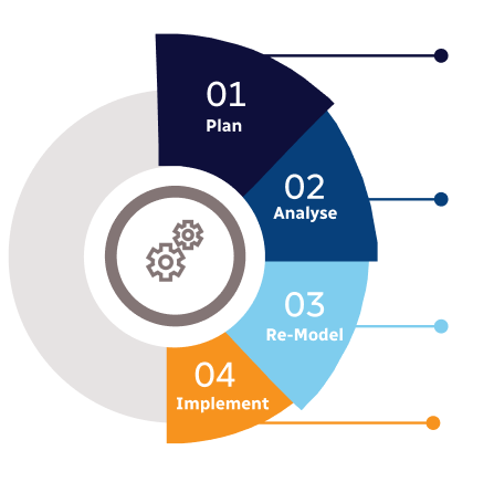
Methodology

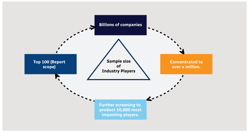
Step 1 - Identification of Relevant Samples Size from Population Database

Step Chart
Bar Chart
Method Chart

Step 2 - Approaches for Defining Global Market Size (Value, Volume* & Price*)

Approach Chart
Top-down and bottom-up approaches are used to validate the global market size and estimate the market size for manufactures, regional segments, product, and application.

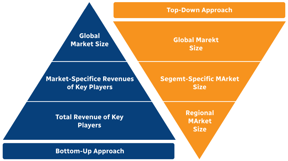
Note*: In applicable scenarios

Step 3 - Data Sources

Primary Research

  • Web Analytics
  • Survey Reports
  • Research Institute
  • Latest Research Reports
  • Opinion Leaders

Secondary Research

  • Annual Reports
  • White Paper
  • Latest Press Release
  • Industry Association
  • Paid Database
  • Investor Presentations
Analyst Chart

Step 4 - Data Triangulation

Involves using different sources of information in order to increase the validity of a study

These sources are likely to be stakeholders in a program - participants, other researchers, program staff, other community members, and so on.

Then we put all data in single framework & apply various statistical tools to find out the dynamic on the market.

During the analysis stage, feedback from the stakeholder groups would be compared to determine areas of agreement as well as areas of divergence

Additionally, after gathering mixed and scattered data from a wide range of sources, data is triangulated and correlated to come up with estimated figures which are further validated through primary mediums or industry experts, opinion leaders.