


Key Insights
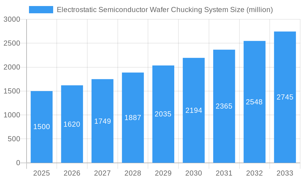
The global Electrostatic Semiconductor Wafer Chucking System market is poised for significant expansion, driven by the escalating demand for advanced semiconductor devices across numerous industries. With a projected market size of approximately USD 1.5 billion in 2025, the industry is expected to witness a robust Compound Annual Growth Rate (CAGR) of around 8% from 2025 to 2033. This growth trajectory is underpinned by the critical role electrostatic chucks play in precision wafer handling during semiconductor manufacturing, ensuring improved yields and reduced defects. The increasing complexity and miniaturization of chips necessitate highly accurate and reliable wafer clamping solutions, directly fueling the adoption of electrostatic chucks. The dominant application segment is anticipated to be 300 mm wafers, reflecting the industry's shift towards larger wafer diameters for enhanced production efficiency and cost-effectiveness. Coulomb-type electrostatic chucks are expected to lead due to their superior holding force and suitability for a wide range of wafer materials. Key players like SHINKO, TOTO, and Applied Materials are actively investing in research and development to offer innovative solutions that meet the evolving demands of semiconductor fabrication.
Electrostatic Semiconductor Wafer Chucking System Market Size (In Billion)

The market's growth is further propelled by key trends such as the increasing adoption of advanced packaging technologies, the burgeoning demand for high-performance computing and artificial intelligence (AI) hardware, and the continuous evolution of consumer electronics. Emerging economies, particularly in the Asia Pacific region (led by China and South Korea), are emerging as significant growth hubs, owing to substantial investments in semiconductor manufacturing infrastructure. While the market presents lucrative opportunities, certain restraints like the high initial investment costs for advanced chuck systems and the need for specialized maintenance could pose challenges. However, the relentless pursuit of technological advancements, including the development of novel materials and improved electrostatic control mechanisms, is expected to mitigate these challenges. The market's future will likely be shaped by innovations that enhance electrostatic holding precision, enable faster wafer transfer, and improve energy efficiency, ensuring continued market relevance and expansion.
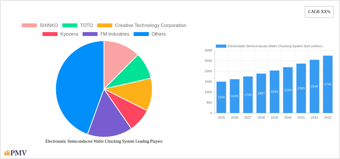
Electrostatic Semiconductor Wafer Chucking System Company Market Share
Electrostatic Semiconductor Wafer Chucking System Market Structure & Competitive Dynamics
The electrostatic semiconductor wafer chucking system market exhibits a dynamic and moderately concentrated competitive landscape. Key players like SHINKO, TOTO, Creative Technology Corporation, Kyocera, FM Industries, NTK CERATEC, Tsukuba Seiko, Applied Materials, and II-VI M Cubed vie for dominance, with market share distribution shifting based on innovation and application specificity. The innovation ecosystem is robust, fueled by continuous R&D in electrostatic chuck technology for enhanced wafer handling precision and defect reduction. Regulatory frameworks, primarily revolving around semiconductor manufacturing standards and material safety, play a crucial role in shaping product development and market entry. Product substitutes, though limited in high-precision applications, include vacuum chucks and mechanical clamps, but electrostatic chucks offer superior advantages in terms of clean handling and reduced particle generation for advanced semiconductor manufacturing. End-user trends, particularly the increasing demand for 300 mm wafers in advanced logic and memory fabrication, are driving market evolution. Mergers and acquisition (M&A) activities, such as potential strategic partnerships between material science providers and equipment manufacturers, are expected to further consolidate the market. While specific M&A deal values are proprietary, strategic acquisitions of smaller, specialized technology firms are anticipated to accelerate innovation and expand market reach. The market is characterized by a strong emphasis on technological advancement and close collaboration with semiconductor manufacturers to meet evolving process requirements.
Electrostatic Semiconductor Wafer Chucking System Industry Trends & Insights
The electrostatic semiconductor wafer chucking system industry is poised for significant expansion, driven by the relentless advancement of semiconductor technology and the escalating demand for higher processing yields. A key growth driver is the transition towards more complex and delicate semiconductor fabrication processes, where electrostatic chucks are indispensable for their ability to hold wafers without mechanical contact, thereby minimizing particulate contamination and wafer damage. This is particularly crucial for the production of advanced logic devices and high-density memory chips. The market penetration of electrostatic chucks is expected to deepen as semiconductor foundries increasingly invest in state-of-the-art manufacturing equipment to meet the exponential growth in data processing, artificial intelligence, and IoT applications. The compound annual growth rate (CAGR) is projected to be substantial, estimated to be around 12-15% over the forecast period, reflecting the critical role these systems play in modern semiconductor manufacturing. Technological disruptions are a constant feature, with ongoing research focused on improving chuck performance, such as enhanced thermal management capabilities, faster response times for wafer placement and removal, and development of chucks compatible with a wider range of wafer materials and sizes, including next-generation wafer substrates. Consumer preferences, in this context, translate to the demands of semiconductor manufacturers for greater efficiency, reliability, and cost-effectiveness in their wafer handling solutions. Competitive dynamics are intense, with established players constantly innovating to offer superior electrostatic chuck solutions. Companies are investing heavily in R&D to develop proprietary technologies that offer enhanced gripping force, better electrostatic field uniformity, and improved durability. The trend towards miniaturization and increased wafer complexity necessitates chucks that can handle smaller features and prevent micro-cracks. Furthermore, the growing emphasis on sustainability in manufacturing is encouraging the development of energy-efficient electrostatic chuck systems. The increasing adoption of advanced packaging techniques also presents new opportunities for electrostatic chucks, as these processes often require precise handling of thinned and fragile wafers. The global push for increased semiconductor self-sufficiency in various regions is also a significant catalyst, leading to increased capital expenditure in wafer fabrication facilities, thereby driving the demand for critical components like electrostatic chucks. The development of smart chucks with integrated sensor technology for real-time monitoring of wafer position and chuck performance is another emerging trend.
Dominant Markets & Segments in Electrostatic Semiconductor Wafer Chucking System
The 300 mm Wafers segment represents the undisputed dominant market within the electrostatic semiconductor wafer chucking system industry. This dominance is primarily driven by the global expansion and technological advancements in leading-edge logic and memory chip manufacturing. Foundries worldwide are heavily invested in 300 mm wafer fabrication facilities to produce high-performance processors, GPUs, and advanced DRAM and NAND flash memory, directly fueling the demand for electrostatic chucks optimized for this wafer diameter. The economic policies and infrastructure development supporting semiconductor manufacturing hubs in North America, East Asia, and Europe are crucial drivers. For instance, government incentives for domestic chip production and the establishment of advanced research and development centers create a fertile ground for the widespread adoption of 300 mm wafer technology and its associated chucking systems.
Within the Types segmentation, Coulomb Type Electrostatic Chucks currently hold a larger market share and are considered the dominant type. This is due to their widespread applicability in a majority of semiconductor manufacturing processes, including lithography, etching, and deposition, where precise and stable wafer holding is paramount. Coulombic attraction, generated by a uniform electric field, provides a strong and stable grip, crucial for preventing wafer movement during high-speed operations. The reliability, maturity of technology, and established manufacturing processes for Coulomb Type chucks contribute to their current market leadership.
However, the Johnsen-Rahbek (JR) Type Electrostatic Chucks are experiencing rapid growth and are projected to capture a significant portion of the market, especially in specialized applications. JR Type chucks offer advantages in situations requiring very low holding forces or for handling highly sensitive wafers, where the risk of electrostatic discharge (ESD) needs to be minimized. Their ability to provide controlled and adjustable gripping forces makes them increasingly valuable for advanced packaging and thinned wafer handling. The increasing complexity of semiconductor devices and the demand for higher yields are driving the adoption of JR Type chucks in niche but high-value applications.
Geographically, East Asia, particularly South Korea and Taiwan, are leading markets for electrostatic semiconductor wafer chucking systems. This is attributable to the presence of the world's largest semiconductor manufacturers, such as Samsung Electronics and TSMC, which operate extensive 300 mm wafer fabrication plants and are at the forefront of adopting advanced manufacturing technologies. The high volume of wafer production and continuous investment in cutting-edge equipment in this region create a robust demand for high-performance electrostatic chucks.
Electrostatic Semiconductor Wafer Chucking System Product Innovations
Product innovations in electrostatic semiconductor wafer chucking systems are primarily focused on enhancing wafer handling precision, minimizing particle generation, and improving thermal management. Developments include the integration of advanced materials for increased durability and electrostatic efficiency, as well as sophisticated control systems for finer gripping force adjustments. These innovations are crucial for meeting the demands of next-generation semiconductor manufacturing, particularly for 300 mm wafers processed with increasingly complex lithography and etching techniques. Competitive advantages are derived from proprietary designs that offer reduced electrostatic discharge risks, faster wafer placement and removal, and extended service life, directly contributing to higher wafer yields and reduced manufacturing costs for semiconductor foundries.
Report Segmentation & Scope
This report segments the electrostatic semiconductor wafer chucking system market across key applications and types. The 300 mm Wafers segment is projected to exhibit the highest market size and growth rate, driven by ongoing investments in advanced semiconductor manufacturing. The 200 mm Wafers segment remains relevant for specialized applications and older fabrication lines, with steady, albeit slower, growth. The Others segment, encompassing smaller wafer sizes and emerging wafer technologies, represents a niche but evolving market. In terms of chuck types, Coulomb Type Electrostatic Chucks currently dominate the market due to their broad applicability and established reliability, while Johnsen-Rahbek (JR) Type Electrostatic Chucks are expected to witness significant growth driven by specialized applications requiring finer control and ESD sensitivity. The scope encompasses the entire value chain, from material suppliers to end-users in the semiconductor industry.
Key Drivers of Electrostatic Semiconductor Wafer Chucking System Growth
The growth of the electrostatic semiconductor wafer chucking system market is propelled by several key drivers. Foremost is the escalating demand for advanced semiconductors, fueled by the expansion of artificial intelligence, 5G technology, and the Internet of Things (IoT), which necessitates higher wafer processing volumes. Technological advancements in chip design, leading to smaller and more complex features, require increasingly precise wafer handling, a critical function of electrostatic chucks. Furthermore, the global trend of increasing semiconductor self-sufficiency and onshoring initiatives is driving substantial investments in new wafer fabrication plants, thereby boosting the demand for essential manufacturing equipment. The continuous drive for higher manufacturing yields and reduced defect rates in semiconductor production also makes electrostatic chucks a preferred choice over alternative holding mechanisms.
Challenges in the Electrostatic Semiconductor Wafer Chucking System Sector
Despite robust growth prospects, the electrostatic semiconductor wafer chucking system sector faces several challenges. The high cost of advanced electrostatic chuck technology can be a barrier for smaller manufacturers or those with limited capital expenditure budgets. Supply chain complexities and the sourcing of specialized raw materials for chuck manufacturing can lead to production bottlenecks and price volatility. Stringent quality control and the need for extremely high reliability in semiconductor manufacturing demand rigorous testing and validation, which can prolong product development cycles. Competitive pressures from established players and the threat of technological obsolescence due to rapid innovation also pose significant challenges. Furthermore, ensuring consistent performance across varying environmental conditions within cleanrooms requires continuous technological refinement.
Leading Players in the Electrostatic Semiconductor Wafer Chucking System Market
- SHINKO
- TOTO
- Creative Technology Corporation
- Kyocera
- FM Industries
- NTK CERATEC
- Tsukuba Seiko
- Applied Materials
- II-VI M Cubed
Key Developments in Electrostatic Semiconductor Wafer Chucking System Sector
- 2023: Introduction of new Coulomb Type electrostatic chucks with enhanced thermal management for advanced deposition processes.
- 2023: Development of highly precise JR Type electrostatic chucks for handling extremely thinned wafers in advanced packaging.
- 2022: Strategic collaboration between a leading chuck manufacturer and a semiconductor equipment supplier to integrate advanced chuck technology into new lithography systems.
- 2021: Launch of electrostatic chucks with improved particle-free operation, addressing critical yield concerns in wafer fabrication.
- 2020: Significant investment in R&D by multiple companies to develop next-generation electrostatic chucks capable of handling larger wafer diameters beyond 300 mm, for future semiconductor nodes.
Strategic Electrostatic Semiconductor Wafer Chucking System Market Outlook
The strategic outlook for the electrostatic semiconductor wafer chucking system market is highly optimistic, characterized by sustained growth driven by ongoing technological advancements and the burgeoning global demand for semiconductors. Future market potential lies in the continuous evolution of electrostatic chuck technology to accommodate increasingly complex wafer processing steps, such as EUV lithography and advanced 3D stacking. Strategic opportunities for market players include expanding their product portfolios to cater to emerging applications like compound semiconductor fabrication and advanced sensor manufacturing. The increasing focus on smart manufacturing and Industry 4.0 also presents an opportunity for the development of integrated, sensor-equipped electrostatic chucks that provide real-time data for process optimization and predictive maintenance. Partnerships and collaborations with semiconductor equipment manufacturers and foundries will be crucial for staying ahead of the technological curve and securing long-term market share.
Electrostatic Semiconductor Wafer Chucking System Segmentation
-
1. Application
- 1.1. 300 mm Wafers
- 1.2. 200 mm Wafers
- 1.3. Others
-
2. Types
- 2.1. Coulomb Type Electrostatic Chucks
- 2.2. Johnsen-Rahbek (JR) Type Electrostatic Chucks
Electrostatic Semiconductor Wafer Chucking System Segmentation By Geography
-
1. North America
- 1.1. United States
- 1.2. Canada
- 1.3. Mexico
-
2. South America
- 2.1. Brazil
- 2.2. Argentina
- 2.3. Rest of South America
-
3. Europe
- 3.1. United Kingdom
- 3.2. Germany
- 3.3. France
- 3.4. Italy
- 3.5. Spain
- 3.6. Russia
- 3.7. Benelux
- 3.8. Nordics
- 3.9. Rest of Europe
-
4. Middle East & Africa
- 4.1. Turkey
- 4.2. Israel
- 4.3. GCC
- 4.4. North Africa
- 4.5. South Africa
- 4.6. Rest of Middle East & Africa
-
5. Asia Pacific
- 5.1. China
- 5.2. India
- 5.3. Japan
- 5.4. South Korea
- 5.5. ASEAN
- 5.6. Oceania
- 5.7. Rest of Asia Pacific
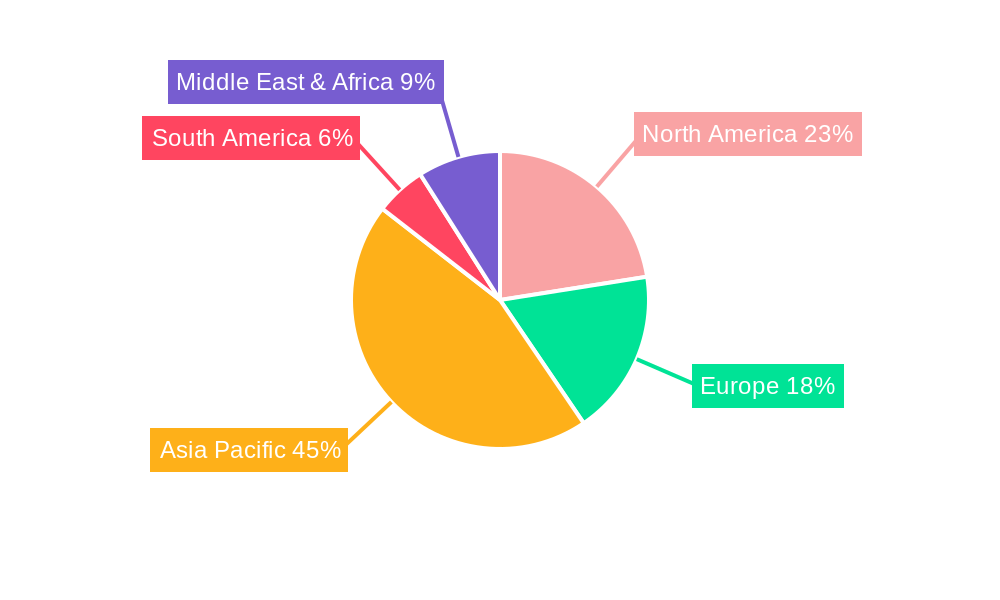
Electrostatic Semiconductor Wafer Chucking System Regional Market Share
Geographic Coverage of Electrostatic Semiconductor Wafer Chucking System
Electrostatic Semiconductor Wafer Chucking System REPORT HIGHLIGHTS
| Aspects | Details |
|---|---|
| Study Period | 2020-2034 |
| Base Year | 2025 |
| Estimated Year | 2026 |
| Forecast Period | 2026-2034 |
| Historical Period | 2020-2025 |
| Growth Rate | CAGR of 5.3% from 2020-2034 |
| Segmentation |
|
Table of Contents
- 1. Introduction
- 1.1. Research Scope
- 1.2. Market Segmentation
- 1.3. Research Methodology
- 1.4. Definitions and Assumptions
- 2. Executive Summary
- 2.1. Introduction
- 3. Market Dynamics
- 3.1. Introduction
- 3.2. Market Drivers
- 3.3. Market Restrains
- 3.4. Market Trends
- 4. Market Factor Analysis
- 4.1. Porters Five Forces
- 4.2. Supply/Value Chain
- 4.3. PESTEL analysis
- 4.4. Market Entropy
- 4.5. Patent/Trademark Analysis
- 5. Global Electrostatic Semiconductor Wafer Chucking System Analysis, Insights and Forecast, 2020-2032
- 5.1. Market Analysis, Insights and Forecast - by Application
- 5.1.1. 300 mm Wafers
- 5.1.2. 200 mm Wafers
- 5.1.3. Others
- 5.2. Market Analysis, Insights and Forecast - by Types
- 5.2.1. Coulomb Type Electrostatic Chucks
- 5.2.2. Johnsen-Rahbek (JR) Type Electrostatic Chucks
- 5.3. Market Analysis, Insights and Forecast - by Region
- 5.3.1. North America
- 5.3.2. South America
- 5.3.3. Europe
- 5.3.4. Middle East & Africa
- 5.3.5. Asia Pacific
- 5.1. Market Analysis, Insights and Forecast - by Application
- 6. North America Electrostatic Semiconductor Wafer Chucking System Analysis, Insights and Forecast, 2020-2032
- 6.1. Market Analysis, Insights and Forecast - by Application
- 6.1.1. 300 mm Wafers
- 6.1.2. 200 mm Wafers
- 6.1.3. Others
- 6.2. Market Analysis, Insights and Forecast - by Types
- 6.2.1. Coulomb Type Electrostatic Chucks
- 6.2.2. Johnsen-Rahbek (JR) Type Electrostatic Chucks
- 6.1. Market Analysis, Insights and Forecast - by Application
- 7. South America Electrostatic Semiconductor Wafer Chucking System Analysis, Insights and Forecast, 2020-2032
- 7.1. Market Analysis, Insights and Forecast - by Application
- 7.1.1. 300 mm Wafers
- 7.1.2. 200 mm Wafers
- 7.1.3. Others
- 7.2. Market Analysis, Insights and Forecast - by Types
- 7.2.1. Coulomb Type Electrostatic Chucks
- 7.2.2. Johnsen-Rahbek (JR) Type Electrostatic Chucks
- 7.1. Market Analysis, Insights and Forecast - by Application
- 8. Europe Electrostatic Semiconductor Wafer Chucking System Analysis, Insights and Forecast, 2020-2032
- 8.1. Market Analysis, Insights and Forecast - by Application
- 8.1.1. 300 mm Wafers
- 8.1.2. 200 mm Wafers
- 8.1.3. Others
- 8.2. Market Analysis, Insights and Forecast - by Types
- 8.2.1. Coulomb Type Electrostatic Chucks
- 8.2.2. Johnsen-Rahbek (JR) Type Electrostatic Chucks
- 8.1. Market Analysis, Insights and Forecast - by Application
- 9. Middle East & Africa Electrostatic Semiconductor Wafer Chucking System Analysis, Insights and Forecast, 2020-2032
- 9.1. Market Analysis, Insights and Forecast - by Application
- 9.1.1. 300 mm Wafers
- 9.1.2. 200 mm Wafers
- 9.1.3. Others
- 9.2. Market Analysis, Insights and Forecast - by Types
- 9.2.1. Coulomb Type Electrostatic Chucks
- 9.2.2. Johnsen-Rahbek (JR) Type Electrostatic Chucks
- 9.1. Market Analysis, Insights and Forecast - by Application
- 10. Asia Pacific Electrostatic Semiconductor Wafer Chucking System Analysis, Insights and Forecast, 2020-2032
- 10.1. Market Analysis, Insights and Forecast - by Application
- 10.1.1. 300 mm Wafers
- 10.1.2. 200 mm Wafers
- 10.1.3. Others
- 10.2. Market Analysis, Insights and Forecast - by Types
- 10.2.1. Coulomb Type Electrostatic Chucks
- 10.2.2. Johnsen-Rahbek (JR) Type Electrostatic Chucks
- 10.1. Market Analysis, Insights and Forecast - by Application
- 11. Competitive Analysis
- 11.1. Global Market Share Analysis 2025
- 11.2. Company Profiles
- 11.2.1 SHINKO
- 11.2.1.1. Overview
- 11.2.1.2. Products
- 11.2.1.3. SWOT Analysis
- 11.2.1.4. Recent Developments
- 11.2.1.5. Financials (Based on Availability)
- 11.2.2 TOTO
- 11.2.2.1. Overview
- 11.2.2.2. Products
- 11.2.2.3. SWOT Analysis
- 11.2.2.4. Recent Developments
- 11.2.2.5. Financials (Based on Availability)
- 11.2.3 Creative Technology Corporation
- 11.2.3.1. Overview
- 11.2.3.2. Products
- 11.2.3.3. SWOT Analysis
- 11.2.3.4. Recent Developments
- 11.2.3.5. Financials (Based on Availability)
- 11.2.4 Kyocera
- 11.2.4.1. Overview
- 11.2.4.2. Products
- 11.2.4.3. SWOT Analysis
- 11.2.4.4. Recent Developments
- 11.2.4.5. Financials (Based on Availability)
- 11.2.5 FM Industries
- 11.2.5.1. Overview
- 11.2.5.2. Products
- 11.2.5.3. SWOT Analysis
- 11.2.5.4. Recent Developments
- 11.2.5.5. Financials (Based on Availability)
- 11.2.6 NTK CERATEC
- 11.2.6.1. Overview
- 11.2.6.2. Products
- 11.2.6.3. SWOT Analysis
- 11.2.6.4. Recent Developments
- 11.2.6.5. Financials (Based on Availability)
- 11.2.7 Tsukuba Seiko
- 11.2.7.1. Overview
- 11.2.7.2. Products
- 11.2.7.3. SWOT Analysis
- 11.2.7.4. Recent Developments
- 11.2.7.5. Financials (Based on Availability)
- 11.2.8 Applied Materials
- 11.2.8.1. Overview
- 11.2.8.2. Products
- 11.2.8.3. SWOT Analysis
- 11.2.8.4. Recent Developments
- 11.2.8.5. Financials (Based on Availability)
- 11.2.9 II-VI M Cubed
- 11.2.9.1. Overview
- 11.2.9.2. Products
- 11.2.9.3. SWOT Analysis
- 11.2.9.4. Recent Developments
- 11.2.9.5. Financials (Based on Availability)
- 11.2.1 SHINKO
List of Figures
- Figure 1: Global Electrostatic Semiconductor Wafer Chucking System Revenue Breakdown (undefined, %) by Region 2025 & 2033
- Figure 2: North America Electrostatic Semiconductor Wafer Chucking System Revenue (undefined), by Application 2025 & 2033
- Figure 3: North America Electrostatic Semiconductor Wafer Chucking System Revenue Share (%), by Application 2025 & 2033
- Figure 4: North America Electrostatic Semiconductor Wafer Chucking System Revenue (undefined), by Types 2025 & 2033
- Figure 5: North America Electrostatic Semiconductor Wafer Chucking System Revenue Share (%), by Types 2025 & 2033
- Figure 6: North America Electrostatic Semiconductor Wafer Chucking System Revenue (undefined), by Country 2025 & 2033
- Figure 7: North America Electrostatic Semiconductor Wafer Chucking System Revenue Share (%), by Country 2025 & 2033
- Figure 8: South America Electrostatic Semiconductor Wafer Chucking System Revenue (undefined), by Application 2025 & 2033
- Figure 9: South America Electrostatic Semiconductor Wafer Chucking System Revenue Share (%), by Application 2025 & 2033
- Figure 10: South America Electrostatic Semiconductor Wafer Chucking System Revenue (undefined), by Types 2025 & 2033
- Figure 11: South America Electrostatic Semiconductor Wafer Chucking System Revenue Share (%), by Types 2025 & 2033
- Figure 12: South America Electrostatic Semiconductor Wafer Chucking System Revenue (undefined), by Country 2025 & 2033
- Figure 13: South America Electrostatic Semiconductor Wafer Chucking System Revenue Share (%), by Country 2025 & 2033
- Figure 14: Europe Electrostatic Semiconductor Wafer Chucking System Revenue (undefined), by Application 2025 & 2033
- Figure 15: Europe Electrostatic Semiconductor Wafer Chucking System Revenue Share (%), by Application 2025 & 2033
- Figure 16: Europe Electrostatic Semiconductor Wafer Chucking System Revenue (undefined), by Types 2025 & 2033
- Figure 17: Europe Electrostatic Semiconductor Wafer Chucking System Revenue Share (%), by Types 2025 & 2033
- Figure 18: Europe Electrostatic Semiconductor Wafer Chucking System Revenue (undefined), by Country 2025 & 2033
- Figure 19: Europe Electrostatic Semiconductor Wafer Chucking System Revenue Share (%), by Country 2025 & 2033
- Figure 20: Middle East & Africa Electrostatic Semiconductor Wafer Chucking System Revenue (undefined), by Application 2025 & 2033
- Figure 21: Middle East & Africa Electrostatic Semiconductor Wafer Chucking System Revenue Share (%), by Application 2025 & 2033
- Figure 22: Middle East & Africa Electrostatic Semiconductor Wafer Chucking System Revenue (undefined), by Types 2025 & 2033
- Figure 23: Middle East & Africa Electrostatic Semiconductor Wafer Chucking System Revenue Share (%), by Types 2025 & 2033
- Figure 24: Middle East & Africa Electrostatic Semiconductor Wafer Chucking System Revenue (undefined), by Country 2025 & 2033
- Figure 25: Middle East & Africa Electrostatic Semiconductor Wafer Chucking System Revenue Share (%), by Country 2025 & 2033
- Figure 26: Asia Pacific Electrostatic Semiconductor Wafer Chucking System Revenue (undefined), by Application 2025 & 2033
- Figure 27: Asia Pacific Electrostatic Semiconductor Wafer Chucking System Revenue Share (%), by Application 2025 & 2033
- Figure 28: Asia Pacific Electrostatic Semiconductor Wafer Chucking System Revenue (undefined), by Types 2025 & 2033
- Figure 29: Asia Pacific Electrostatic Semiconductor Wafer Chucking System Revenue Share (%), by Types 2025 & 2033
- Figure 30: Asia Pacific Electrostatic Semiconductor Wafer Chucking System Revenue (undefined), by Country 2025 & 2033
- Figure 31: Asia Pacific Electrostatic Semiconductor Wafer Chucking System Revenue Share (%), by Country 2025 & 2033
List of Tables
- Table 1: Global Electrostatic Semiconductor Wafer Chucking System Revenue undefined Forecast, by Application 2020 & 2033
- Table 2: Global Electrostatic Semiconductor Wafer Chucking System Revenue undefined Forecast, by Types 2020 & 2033
- Table 3: Global Electrostatic Semiconductor Wafer Chucking System Revenue undefined Forecast, by Region 2020 & 2033
- Table 4: Global Electrostatic Semiconductor Wafer Chucking System Revenue undefined Forecast, by Application 2020 & 2033
- Table 5: Global Electrostatic Semiconductor Wafer Chucking System Revenue undefined Forecast, by Types 2020 & 2033
- Table 6: Global Electrostatic Semiconductor Wafer Chucking System Revenue undefined Forecast, by Country 2020 & 2033
- Table 7: United States Electrostatic Semiconductor Wafer Chucking System Revenue (undefined) Forecast, by Application 2020 & 2033
- Table 8: Canada Electrostatic Semiconductor Wafer Chucking System Revenue (undefined) Forecast, by Application 2020 & 2033
- Table 9: Mexico Electrostatic Semiconductor Wafer Chucking System Revenue (undefined) Forecast, by Application 2020 & 2033
- Table 10: Global Electrostatic Semiconductor Wafer Chucking System Revenue undefined Forecast, by Application 2020 & 2033
- Table 11: Global Electrostatic Semiconductor Wafer Chucking System Revenue undefined Forecast, by Types 2020 & 2033
- Table 12: Global Electrostatic Semiconductor Wafer Chucking System Revenue undefined Forecast, by Country 2020 & 2033
- Table 13: Brazil Electrostatic Semiconductor Wafer Chucking System Revenue (undefined) Forecast, by Application 2020 & 2033
- Table 14: Argentina Electrostatic Semiconductor Wafer Chucking System Revenue (undefined) Forecast, by Application 2020 & 2033
- Table 15: Rest of South America Electrostatic Semiconductor Wafer Chucking System Revenue (undefined) Forecast, by Application 2020 & 2033
- Table 16: Global Electrostatic Semiconductor Wafer Chucking System Revenue undefined Forecast, by Application 2020 & 2033
- Table 17: Global Electrostatic Semiconductor Wafer Chucking System Revenue undefined Forecast, by Types 2020 & 2033
- Table 18: Global Electrostatic Semiconductor Wafer Chucking System Revenue undefined Forecast, by Country 2020 & 2033
- Table 19: United Kingdom Electrostatic Semiconductor Wafer Chucking System Revenue (undefined) Forecast, by Application 2020 & 2033
- Table 20: Germany Electrostatic Semiconductor Wafer Chucking System Revenue (undefined) Forecast, by Application 2020 & 2033
- Table 21: France Electrostatic Semiconductor Wafer Chucking System Revenue (undefined) Forecast, by Application 2020 & 2033
- Table 22: Italy Electrostatic Semiconductor Wafer Chucking System Revenue (undefined) Forecast, by Application 2020 & 2033
- Table 23: Spain Electrostatic Semiconductor Wafer Chucking System Revenue (undefined) Forecast, by Application 2020 & 2033
- Table 24: Russia Electrostatic Semiconductor Wafer Chucking System Revenue (undefined) Forecast, by Application 2020 & 2033
- Table 25: Benelux Electrostatic Semiconductor Wafer Chucking System Revenue (undefined) Forecast, by Application 2020 & 2033
- Table 26: Nordics Electrostatic Semiconductor Wafer Chucking System Revenue (undefined) Forecast, by Application 2020 & 2033
- Table 27: Rest of Europe Electrostatic Semiconductor Wafer Chucking System Revenue (undefined) Forecast, by Application 2020 & 2033
- Table 28: Global Electrostatic Semiconductor Wafer Chucking System Revenue undefined Forecast, by Application 2020 & 2033
- Table 29: Global Electrostatic Semiconductor Wafer Chucking System Revenue undefined Forecast, by Types 2020 & 2033
- Table 30: Global Electrostatic Semiconductor Wafer Chucking System Revenue undefined Forecast, by Country 2020 & 2033
- Table 31: Turkey Electrostatic Semiconductor Wafer Chucking System Revenue (undefined) Forecast, by Application 2020 & 2033
- Table 32: Israel Electrostatic Semiconductor Wafer Chucking System Revenue (undefined) Forecast, by Application 2020 & 2033
- Table 33: GCC Electrostatic Semiconductor Wafer Chucking System Revenue (undefined) Forecast, by Application 2020 & 2033
- Table 34: North Africa Electrostatic Semiconductor Wafer Chucking System Revenue (undefined) Forecast, by Application 2020 & 2033
- Table 35: South Africa Electrostatic Semiconductor Wafer Chucking System Revenue (undefined) Forecast, by Application 2020 & 2033
- Table 36: Rest of Middle East & Africa Electrostatic Semiconductor Wafer Chucking System Revenue (undefined) Forecast, by Application 2020 & 2033
- Table 37: Global Electrostatic Semiconductor Wafer Chucking System Revenue undefined Forecast, by Application 2020 & 2033
- Table 38: Global Electrostatic Semiconductor Wafer Chucking System Revenue undefined Forecast, by Types 2020 & 2033
- Table 39: Global Electrostatic Semiconductor Wafer Chucking System Revenue undefined Forecast, by Country 2020 & 2033
- Table 40: China Electrostatic Semiconductor Wafer Chucking System Revenue (undefined) Forecast, by Application 2020 & 2033
- Table 41: India Electrostatic Semiconductor Wafer Chucking System Revenue (undefined) Forecast, by Application 2020 & 2033
- Table 42: Japan Electrostatic Semiconductor Wafer Chucking System Revenue (undefined) Forecast, by Application 2020 & 2033
- Table 43: South Korea Electrostatic Semiconductor Wafer Chucking System Revenue (undefined) Forecast, by Application 2020 & 2033
- Table 44: ASEAN Electrostatic Semiconductor Wafer Chucking System Revenue (undefined) Forecast, by Application 2020 & 2033
- Table 45: Oceania Electrostatic Semiconductor Wafer Chucking System Revenue (undefined) Forecast, by Application 2020 & 2033
- Table 46: Rest of Asia Pacific Electrostatic Semiconductor Wafer Chucking System Revenue (undefined) Forecast, by Application 2020 & 2033
Frequently Asked Questions
1. What is the projected Compound Annual Growth Rate (CAGR) of the Electrostatic Semiconductor Wafer Chucking System?
The projected CAGR is approximately 5.3%.
2. Which companies are prominent players in the Electrostatic Semiconductor Wafer Chucking System?
Key companies in the market include SHINKO, TOTO, Creative Technology Corporation, Kyocera, FM Industries, NTK CERATEC, Tsukuba Seiko, Applied Materials, II-VI M Cubed.
3. What are the main segments of the Electrostatic Semiconductor Wafer Chucking System?
The market segments include Application, Types.
4. Can you provide details about the market size?
The market size is estimated to be USD XXX N/A as of 2022.
5. What are some drivers contributing to market growth?
N/A
6. What are the notable trends driving market growth?
N/A
7. Are there any restraints impacting market growth?
N/A
8. Can you provide examples of recent developments in the market?
N/A
9. What pricing options are available for accessing the report?
Pricing options include single-user, multi-user, and enterprise licenses priced at USD 4900.00, USD 7350.00, and USD 9800.00 respectively.
10. Is the market size provided in terms of value or volume?
The market size is provided in terms of value, measured in N/A.
11. Are there any specific market keywords associated with the report?
Yes, the market keyword associated with the report is "Electrostatic Semiconductor Wafer Chucking System," which aids in identifying and referencing the specific market segment covered.
12. How do I determine which pricing option suits my needs best?
The pricing options vary based on user requirements and access needs. Individual users may opt for single-user licenses, while businesses requiring broader access may choose multi-user or enterprise licenses for cost-effective access to the report.
13. Are there any additional resources or data provided in the Electrostatic Semiconductor Wafer Chucking System report?
While the report offers comprehensive insights, it's advisable to review the specific contents or supplementary materials provided to ascertain if additional resources or data are available.
14. How can I stay updated on further developments or reports in the Electrostatic Semiconductor Wafer Chucking System?
To stay informed about further developments, trends, and reports in the Electrostatic Semiconductor Wafer Chucking System, consider subscribing to industry newsletters, following relevant companies and organizations, or regularly checking reputable industry news sources and publications.
Methodology
Step 1 - Identification of Relevant Samples Size from Population Database


Step 2 - Approaches for Defining Global Market Size (Value, Volume* & Price*)

Note*: In applicable scenarios
Step 3 - Data Sources
Primary Research
- Web Analytics
- Survey Reports
- Research Institute
- Latest Research Reports
- Opinion Leaders
Secondary Research
- Annual Reports
- White Paper
- Latest Press Release
- Industry Association
- Paid Database
- Investor Presentations

Step 4 - Data Triangulation
Involves using different sources of information in order to increase the validity of a study
These sources are likely to be stakeholders in a program - participants, other researchers, program staff, other community members, and so on.
Then we put all data in single framework & apply various statistical tools to find out the dynamic on the market.
During the analysis stage, feedback from the stakeholder groups would be compared to determine areas of agreement as well as areas of divergence